News Posts matching #SK Hynix

Return to Keyword Browsing

NVIDIA Devouring Chips Faster than South Korea's Supply, Lowest Inventory in 10 Years

South Korea's stock of semiconductor chips dropped more than it has since 2014. This big decrease shows that customers are buying chips faster than companies can make them, as they need more equipment for developing artificial intelligence (AI) technology. Official data released on May 31 revealed that in April, chip inventories fell by 33.7% compared to a year earlier - the largest drop since late 2014. This is the fourth month in a row that inventories have declined, while at the same time South Korea's exports of semiconductors have gone up again. Additionally, South Korea's production of chips rose 22.3% in April, which is less than the 30.2% increase from the previous month. Shipments from factories grew 18.6%, also lower than March's 16.4% growth.

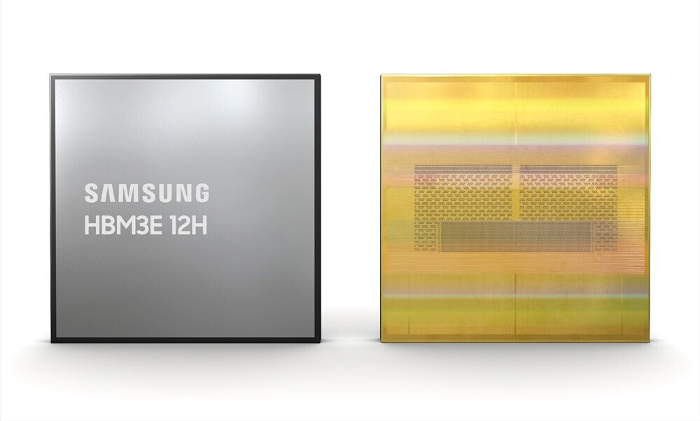
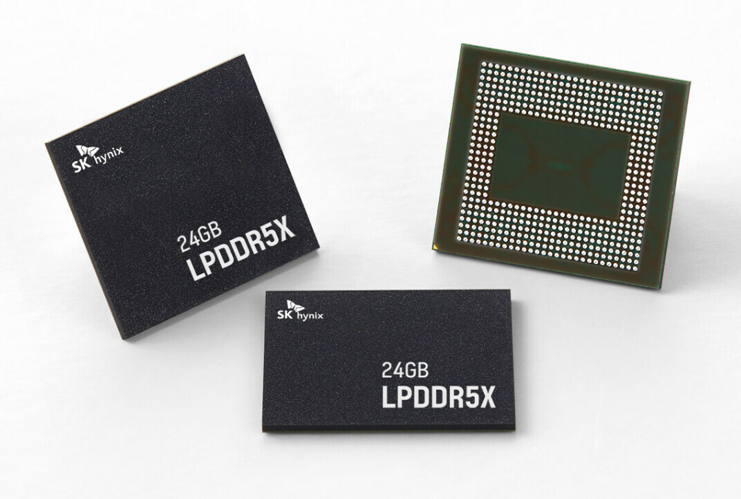
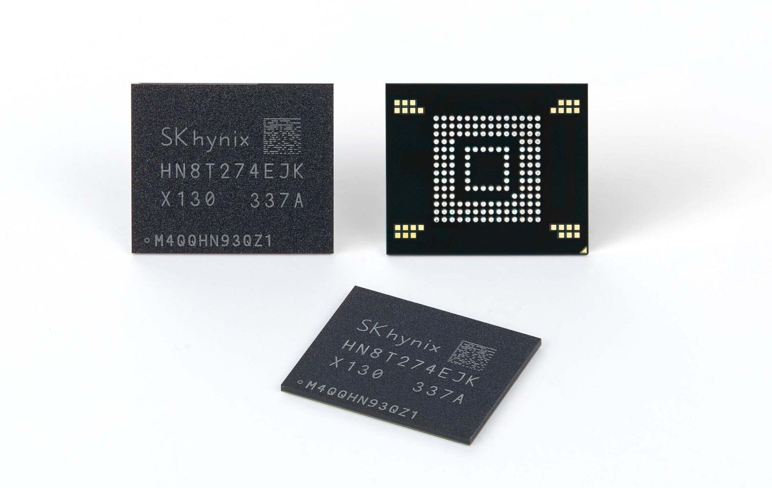
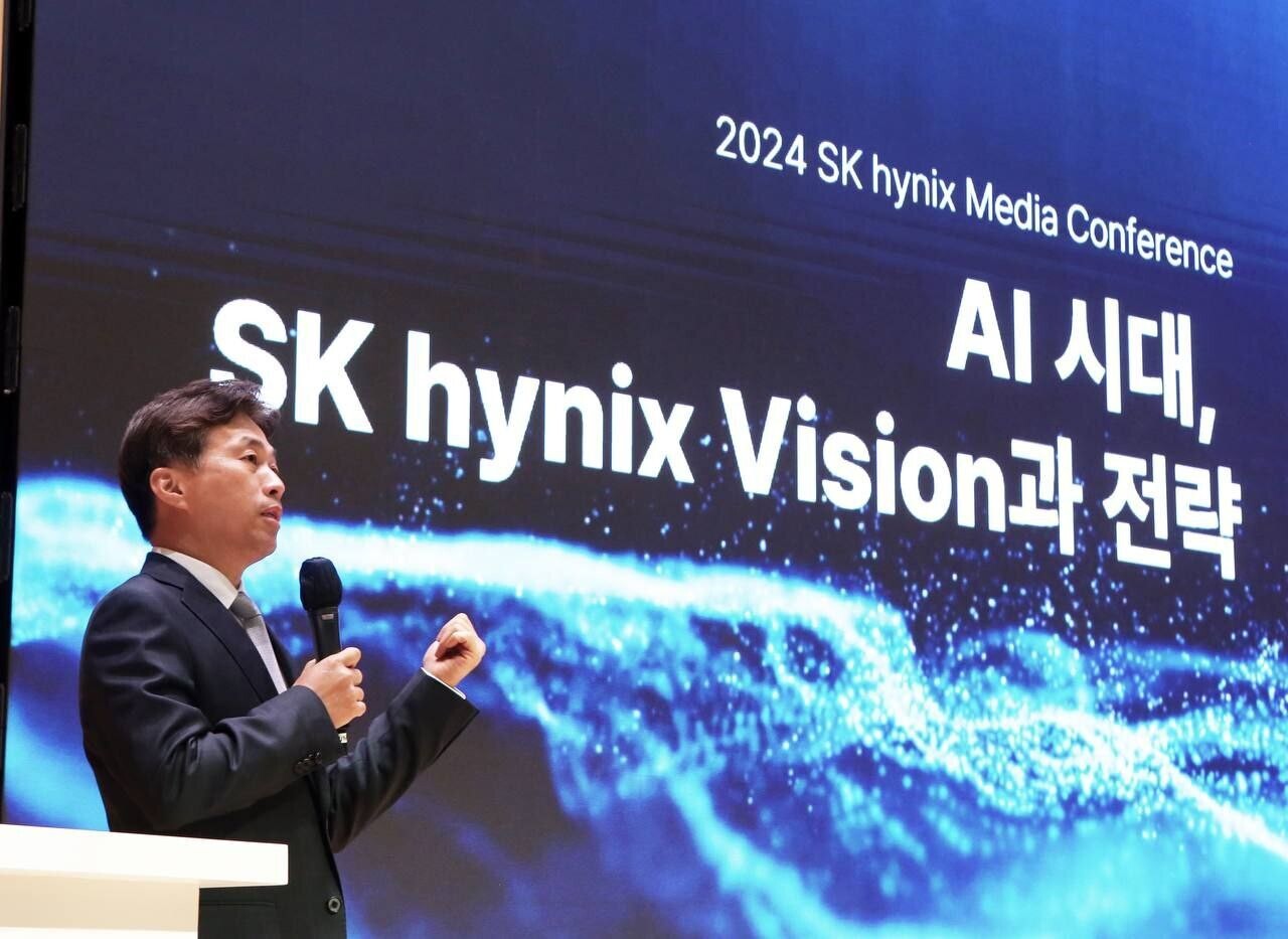
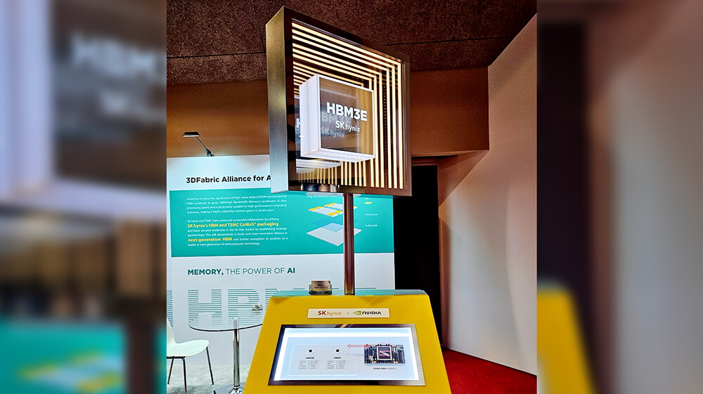
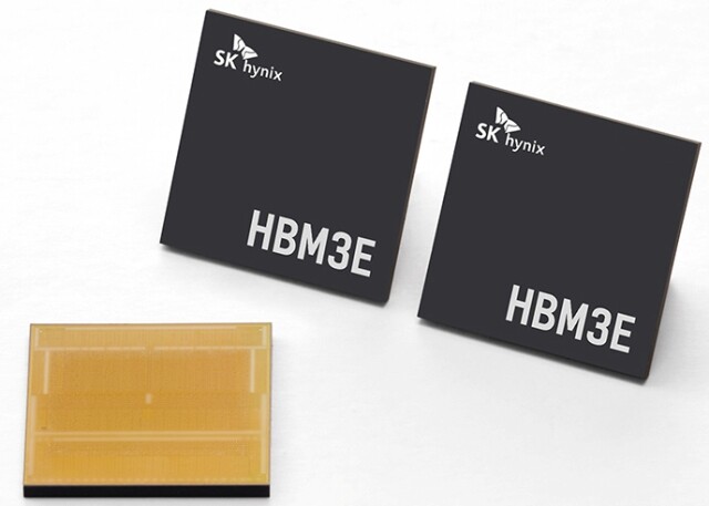
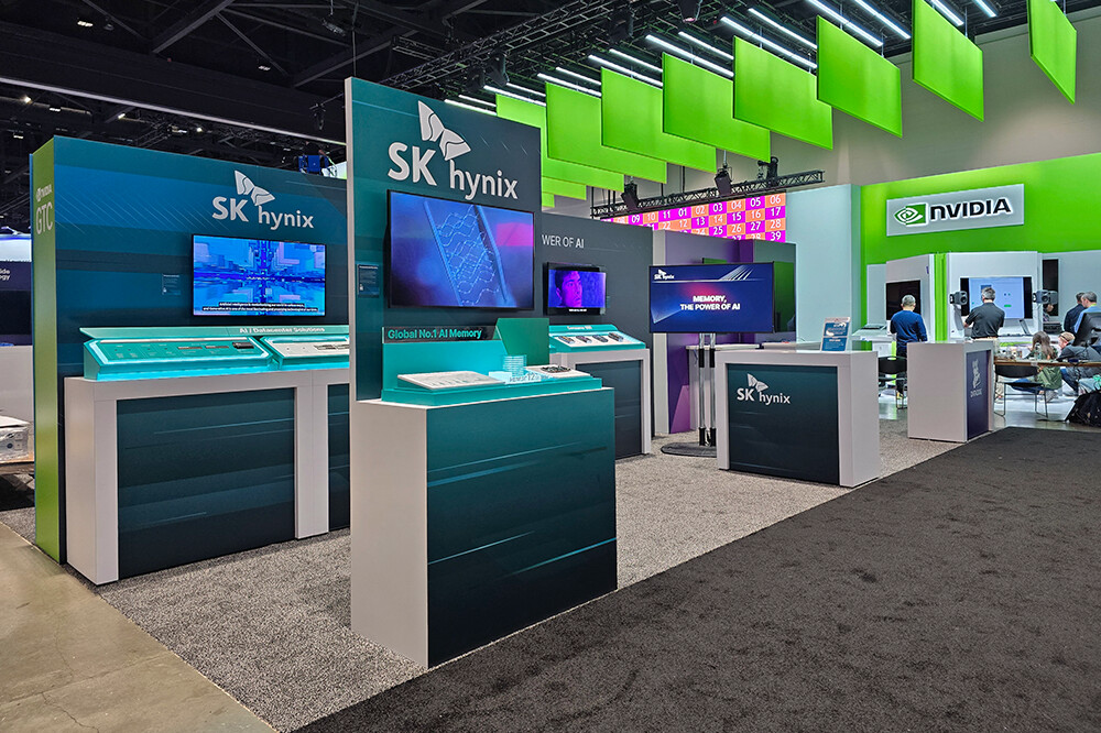
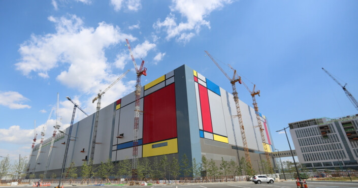
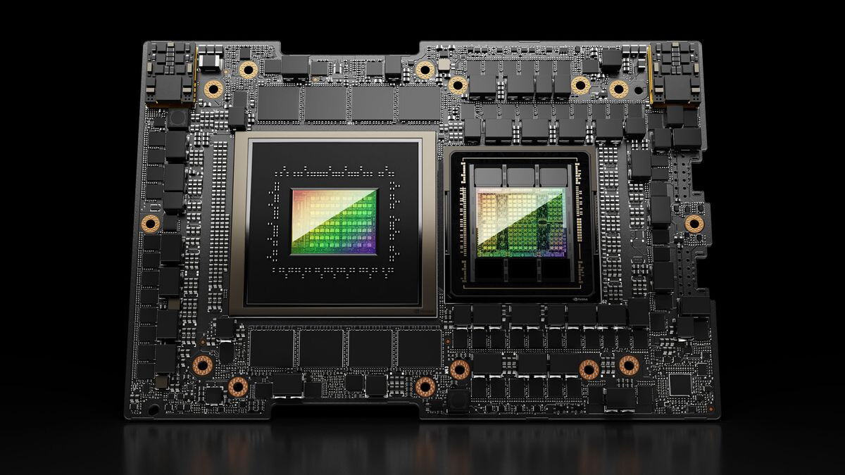
South Korea is home to the two biggest memory chipmakers in the world (Samsung and SK Hynix), and they are competing to supply chips to NVIDIA, the latest having an insatiable appetite for more and more chips. These two Korean companies are in a race to develop a more advanced and more profitable version of high-bandwidth memory, or HBM. During the memory chip boom from 2013-2015, inventories didn't increase for about a year and a half. In the 2016-2017 cycle, inventory declines lasted nearly a year. A report from South Korea's central bank expects the latest surge in chip demand to continue at least until the first half of next year. This is because the "artificial intelligence boom" is driving up demand similarly to how cloud servers caused an expansion in 2016, and now mostly forgotten crypto-mining fever. South Korea will release its latest export data on June 1.
NVIDIA Chips South Korea South Korea Chips Inventory April 2024

Growing Demand for High-Capacity Storage Propels Enterprise SSD Revenue Up by Over 60% in 1Q24

TrendForce reports that a reduction in supplier production has led to unmet demand for high-capacity orders since 4Q23. Combined with procurement strategies aimed at building low-cost inventory, this has driven orders and significantly boosted enterprise SSD revenue, which reached US$3.758 billion in 1Q24—a staggering 62.9% QoQ increase.

TrendForce further highlights that demand for high-capacity, driven by AI servers, has surged. North American clients increasingly adopt high-capacity QLC SSDs to replace HDDs, leading to over 20% growth in Q2 enterprise SSD bit procurement. This has also driven up Q2 enterprise SSD contract prices by more than 20%, with revenue expected to grow by another 20%.

Details Revealed about SK Hynix HBM4E, Computing, and Caching Features Integrated Directly

SK Hynix, leader in HBM3E memory, has now shared more details about HBM4E. Based on fresh reports by Wccftech and ET News, SK Hynix plans to make an HBM memory type that features multiple things like computing, caching, and network memory, all within the same package. This will make SK Hynix stand out from others. This idea is still in the early stages, but SK Hynix has started getting the design information it needs to support its goals. The reports say that SK Hynix wants to lay the groundwork for a versatile HBM with its upcoming HBM4 design. The company reportedly plans to include a memory controller on board, which will allow new computing abilities with its 7th generation HBM4E memory.

By using SK Hynix's method, everything will be unified as a single unit. This will not only make data transfer faster because there is less space between parts, but it will also make it more energy-efficient. Previously in April, SK Hynix announced that it has been working with TSMC to produce the next generation of HBM and improve how logic chips and HBM work together through advanced packaging. In late May, SK Hynix has disclosed yield details regarding HBM3E for the first time, the memory giant reporting successfully reducing the time needed for mass production of HBM3E chips by 50%, while getting closer to the target yield of 80%. The company plans to keep developing HBM4, which is expected to start mass production in 2026.
SK Hynix HBM SK Hynix HBMe3

Micron DRAM Production Plant in Japan Faces Two-Year Delay to 2027

Last year, Micron unveiled plans to construct a cutting-edge DRAM factory in Hiroshima, Japan. However, the project has faced a significant two-year delay, pushing back the initial timeline for mass production of the company's most advanced memory products. Originally slated to begin mass production by the end of 2025, Micron now aims to have the new facility operational by 2027. The complexity of integrating extreme ultraviolet lithography (EUV) equipment, which enables the production of highly advanced chips, has contributed to the delay. The Hiroshima plant will produce next-generation 1-gamma DRAM and high-bandwidth memory (HBM) designed for generative AI applications. Micron expects the HBM market, currently dominated by rivals SK Hynix and Samsung, to experience rapid growth, with the company targeting a 25% market share by 2025.

The project is expected to cost between 600 and 800 billion Japanese yen ($3.8 to $5.1 billion), with Japan's government covering one-third of the cost. Micron has received a subsidy of up to 192 billion yen ($1.2 billion) for construction and equipment, as well as a subsidy to cover half of the necessary funding to produce HBM at the plant, amounting to 25 billion yen ($159 million). Despite the delay, the increased investment in the factory reflects Micron's commitment to advancing its memory technology and capitalizing on the growing demand for HBM. An indication of that is the fact that customers have pre-ordered 100% of the HBM capacity for 2024, not leaving a single HBM die unused.

NAND Flash Industry Revenue Grew 28.1% in 1Q24, Growth Expected to Continue into Q2

TrendForce reports that adoption of enterprise SSDs by AI servers began in February, which subsequently led to large orders. Additionally, PC and smartphone customers have been increasing their inventory levels to manage rising prices. This trend drove up NAND Flash prices and shipment levels in 1Q24 and boosted quarterly revenue by 28.1% to US$14.71 billion.

There were significant changes in market rankings this quarter, with Micron overtaking Western Digital to claim the fourth spot. Micron benefited from slightly lower prices and shipments than its competitors in 4Q23, resulting in a 51.2% QoQ revenue growth to $1.72 billion in 1Q24—the highest among its peers.

NVIDIA Reportedly Having Issues with Samsung's HBM3 Chips Running Too Hot

According to Reuters, NVIDIA is having some major issues with Samsung's HBM3 chips, as NVIDIA hasn't managed to finalise its validations of the chips. Reuters are citing multiple sources that are familiar with the matter and it seems like Samsung is having some serious issues with its HMB3 chips if the sources are correct. Not only do the chips run hot, which itself is a big issue due to NVIDIA already having issues cooling some of its higher-end products, but the power consumption is apparently not where it should be either. Samsung is said to have tried to get its HBM3 and HBM3E parts validated by NVIDIA since sometime in 2023 according to Reuter's sources, which suggests that there have been issues for at least six months, if not longer.

The sources claim there are issues with both the 8- and 12-layer stacks of HMB3E parts from Samsung, suggesting that NVIDIA might only be able to supply parts from Micron and SK Hynix for now, the latter whom has been supplying HBM3 chips to NVIDIA since the middle of 2022 and HBM3E chips since March of this year. It's unclear if this is a production issue at Samsung's DRAM Fabs, a packaging related issue or something else entirely. The Reuter's piece goes on to speculating about Samsung not having had enough time to develop its HBM parts compared its competitors and that it's a rushed product, but Samsung issued a statement to the publication that it's a matter of customising the product for its customer's needs. Samsung also said that it's "the process of optimising its products through close collaboration with customers" without going into which customer(s). Samsung issued a further statement saying that "claims of failing due to heat and power consumption are not true" and that testing was going as expected.

HBM3e Production Surge Expected to Make Up 35% of Advanced Process Wafer Input by End of 2024

TrendForce reports that the three largest DRAM suppliers are increasing wafer input for advanced processes. Following a rise in memory contract prices, companies have boosted their capital investments, with capacity expansion focusing on the second half of this year. It is expected that wafer input for 1alpha nm and above processes will account for approximately 40% of total DRAM wafer input by the end of the year.

HBM production will be prioritized due to its profitability and increasing demand. However, limited yields of around 50-60% and a wafer area 60% larger than DRAM products mean a higher proportion of wafer input is required. Based on the TSV capacity of each company, HBM is expected to account for 35% of advanced process wafer input by the end of this year, with the remaining wafer capacity used for LPDDR5(X) and DDR5 products.

TSMC Unveils Next-Generation HBM4 Base Dies, Built on 12 nm and 5 nm Nodes

During the European Technology Symposium 2024, TSMC has announced its readiness to manufacture next-generation HBM4 base dies using both 12 nm and 5 nm nodes. This significant development is expected to substantially improve the performance, power consumption, and logic density of HBM4 memory, catering to the demands of high-performance computing (HPC) and artificial intelligence (AI) applications. The shift from a traditional 1024-bit interface to an ultra-wide 2048-bit interface is a key aspect of the new HBM4 standard. This change will enable the integration of more logic and higher performance while reducing power consumption. TSMC's N12FFC+ and N5 processes will be used to produce these base dies, with the N12FFC+ process offering a cost-effective solution for achieving HBM4 performance and the N5 process providing even more logic and lower power consumption at HBM4 speeds.

The company is collaborating with major HBM memory partners, including Micron, Samsung, and SK Hynix, to integrate advanced nodes for HBM4 full-stack integration. TSMC's base die, fabricated using the N12FFC+ process, will be used to install HBM4 memory stacks on a silicon interposer alongside system-on-chips (SoCs). This setup will enable the creation of 12-Hi (48 GB) and 16-Hi (64 GB) stacks with per-stack bandwidth exceeding 2 TB/s. TSMC's collaboration with EDA partners like Cadence, Synopsys, and Ansys ensures the integrity of HBM4 channel signals, thermal accuracy, and electromagnetic interference (EMI) in the new HBM4 base dies. TSMC is also optimizing CoWoS-L and CoWoS-R for HBM4 integration, meaning that massive high-performance chips are already utilizing this technology and getting ready for volume manufacturing.

SK hynix Develops Next-Generation Mobile NAND Solution ZUFS 4.0

SK hynix announced today that it has developed the Zoned UFS, or ZUFS 4.0, a mobile NAND solution product for on-device AI applications. SK hynix said that the ZUFS 4.0, optimized for on-device AI from mobile devices such as smartphones, is the industry's best of its kind. The company expects the latest product to help expand its AI memory leadership to the NAND space, extending its success in the high-performance DRAM represented by HBM.

The ZUFS is a differentiated technology that classifies and stores data generated from smartphones in different zones in accordance with characteristics. Unlike a conventional UFS, the latest product groups and stores data with similar purposes and frequencies in separate zones, boosting the speed of a smartphone's operating system and management efficiency of the storage devices.

SK hynix Presents CXL Memory Solutions Set to Power the AI Era at CXL DevCon 2024

SK hynix participated in the first-ever Compute Express Link Consortium Developers Conference (CXL DevCon) held in Santa Clara, California from April 30-May 1. Organized by a group of more than 240 global semiconductor companies known as the CXL Consortium, CXL DevCon 2024 welcomed a majority of the consortium's members to showcase their latest technologies and research results.

CXL is a technology that unifies the interfaces of different devices in a system such as semiconductor memory, storage, and logic chips. As it can increase system bandwidth and processing capacity, CXL is receiving attention as a key technology for the AI era in which high performance and capacity are essential. Under the slogan "Memory, The Power of AI," SK hynix showcased a range of CXL products at the conference that are set to strengthen the company's leadership in AI memory technology.

SK hynix CEO Says HBM from 2025 Production Almost Sold Out

SK hynix held a press conference unveiling its vision and strategy for the AI era today at its headquarters in Icheon, Gyeonggi Province, to share the details of its investment plans for the M15X fab in Cheongju and the Yongin Semiconductor Cluster in Korea and the advanced packaging facilities in Indiana, U.S.

The event, hosted by theChief Executive Officer Kwak Noh-Jung, three years before the May 2027 completion of the first fab in the Yongin Cluster, was attended by key executives including the Head of AI Infra Justin (Ju-Seon) Kim, Head of DRAM Development Kim Jonghwan, Head of the N-S Committee Ahn Hyun, Head of Manufacturing Technology Kim Yeongsik, Head of Package & Test Choi Woojin, Head of Corporate Strategy & Planning Ryu Byung Hoon, and the Chief Financial Officer Kim Woo Hyun.

SK hynix Strengthens AI Memory Leadership & Partnership With Host at the TSMC 2024 Tech Symposium

SK hynix showcased its next-generation technologies and strengthened key partnerships at the TSMC 2024 Technology Symposium held in Santa Clara, California on April 24. At the event, the company displayed its industry-leading HBM AI memory solutions and highlighted its collaboration with TSMC involving the host's CoWoS advanced packaging technology.

TSMC, a global semiconductor foundry, invites its major partners to this annual conference in the first half of each year so they can share their new products and technologies. Attending the event under the slogan "Memory, the Power of AI," SK hynix received significant attention for presenting the industry's most powerful AI memory solution, HBM3E. The product has recently demonstrated industry-leading performance, achieving input/output (I/O) transfer speed of up to 10 gigabits per second (Gbps) in an AI system during a performance validation evaluation.

SK Hynix Announces 1Q24 Financial Results

SK hynix Inc. announced today that it recorded 12.43 trillion won in revenues, 2.886 trillion won in operating profit (with an operating margin of 23%), and 1.917 trillion won in net profit (with a net margin of 15%) in the first quarter. With revenues marking an all-time high for a first quarter and the operating profit a second-highest following the records of the first quarter of 2018, SK hynix believes that it has entered the phase of a clear rebound following a prolonged downturn.

The company said that an increase in the sales of AI server products backed by its leadership in AI memory technology including HBM and continued efforts to prioritize profitability led to a 734% on-quarter jump in the operating profit. With the sales ratio of eSSD, a premium product, on the rise and the average selling prices rising, the NAND business has also achieved a meaningful turnaround in the same period.

SK hynix to Produce DRAM from M15X in Cheongju

SK hynix Inc. announced today that it plans to expand production capacity of the next-generation DRAM including HBM, a core component of the AI infrastructure, in response to the rapidly increasing demand for AI semiconductors. As the board of directors approves the plan, the company will build the M15X fab in Cheongju, North Chungcheong Province, for a new DRAM production base, and invest about 5.3 trillion won for fab construction.

The company plans to start construction at the end of April with an aim to complete in November 2025 for an early mass production. With a gradual increase in equipment investment planned, the total investment in building the new production base will be more than 20 trillion won in the long-term. As a global leader in AI memory, SK hynix expects the expansion in investment to contribute to revitalizing the domestic economy, while refreshing Korea's reputation as a semiconductor powerhouse.

SK hynix Collaborates with TSMC on HBM4 Chip Packaging

SK hynix Inc. announced today that it has recently signed a memorandum of understanding with TSMC for collaboration to produce next-generation HBM and enhance logic and HBM integration through advanced packaging technology. The company plans to proceed with the development of HBM4, or the sixth generation of the HBM family, slated to be mass-produced from 2026, through this initiative.

SK hynix said the collaboration between the global leader in the AI memory space and TSMC, a top global logic foundry, will lead to more innovations in HBM technology. The collaboration is also expected to enable breakthroughs in memory performance through trilateral collaboration between product design, foundry, and memory provider. The two companies will first focus on improving the performance of the base die that is mounted at the very bottom of the HBM package. HBM is made by stacking a core DRAM die on top of a base die that features TSV technology, and vertically connecting a fixed number of layers in the DRAM stack to the core die with TSV into an HBM package. The base die located at the bottom is connected to the GPU, which controls the HBM.

SK hynix Signs Investment Agreement of Advanced Chip Packaging with Indiana

SK hynix Inc., the world's leading producer of High-Bandwidth Memory (HBM) chips, announced today that it will invest an estimated $3.87 billion in West Lafayette, Indiana to build an advanced packaging fabrication and R&D facility for AI products. The project, the first of its kind in the United States, is expected to drive innovation in the nation's AI supply chain, while bringing more than a thousand new jobs to the region.

The company held an investment agreement ceremony with officials from Indiana State, Purdue University, and the U.S. government at Purdue University in West Lafayette on the 3rd and officially announced the plan. At the event, officials from each party including Governor of Indiana Eric Holcomb, Senator Todd Young, Director of the White House Office of Science and Technology Policy Arati Prabhakar, Assistant Secretary of Commerce Arun Venkataraman, Secretary of Commerce State of Indiana David Rosenberg, Purdue University President Mung Chiang, Chairman of Purdue Research Foundation Mitch Daniels, Mayor of city of West Lafayette Erin Easter, Ambassador of the Republic of Korea to the United States Hyundong Cho, Consul General of the Republic of Korea in Chicago Junghan Kim, SK vice chairman Jeong Joon Yu, SK hynix CEO Kwak Noh-Jung and SK hynix Head of Package & Test Choi Woojin, participated.

SK Hynix Plans a $4 Billion Chip Packaging Facility in Indiana

SK Hynix is planning a large $4 billion chip-packaging and testing facility in Indiana, USA. The company is still in the planning stage of the decision to invest in the US. "[the company] is reviewing its advanced chip packaging investment in the US, but hasn't made a final decision yet," a company spokesperson told the Wall Street Journal. The primary product focus for this plant will be stacked HBM memory meant to be consumed by the AI GPU and self-driving automobile industries. The plant could also focus on other exotic memory types, such as high-density server memory; and perhaps even compute-in-memory. The plant is expected to start operations in 2028, and will create up to 1,000 skilled jobs. SK Hynix is counting for state- and federal tax incentives to propel this investment; under government initiatives such as the CHIPS Act. SK Hynix is a significant supplier of HBM to NVIDIA for its AI GPUs. Its HBM3E features in the latest NVIDIA "Blackwell" GPUs.

SK hynix Presents the Future of AI Memory Solutions at NVIDIA GTC 2024

SK hynix is displaying its latest AI memory technologies at NVIDIA's GPU Technology Conference (GTC) 2024 held in San Jose from March 18-21. The annual AI developer conference is proceeding as an in-person event for the first time since the start of the pandemic, welcoming industry officials, tech decision makers, and business leaders. At the event, SK hynix is showcasing new memory solutions for AI and data centers alongside its established products.

Showcasing the Industry's Highest Standard of AI Memory
The AI revolution has continued to pick up pace as AI technologies spread their reach into various industries. In response, SK hynix is developing AI memory solutions capable of handling the vast amounts of data and processing power required by AI. At GTC 2024, the company is displaying some of these products, including its 12-layer HBM3E and Compute Express Link (CXL)1, under the slogan "Memory, The Power of AI". HBM3E, the fifth generation of HBM2, is the highest-specification DRAM for AI applications on the market. It offers the industry's highest capacity of 36 gigabytes (GB), a processing speed of 1.18 terabytes (TB) per second, and exceptional heat dissipation, making it particularly suitable for AI systems. On March 19, SK hynix announced it had become the first in the industry to mass-produce HBM3E.

SK hynix Platinum P51 14 GB/s PCIe Gen 5 SSD Revealed

SK hynix press release about its upcoming PCB01 PCIe 5.0 SSD was a bit light on details and Anandtech got a closer look at the upcoming drive at GTC 2024. Not entirely unsurprising, the drive will be called the Platinum P51 rather than the PCB01, which is a continuation of the branding SK hynix is using for its current range of SSDs. As we already know, it'll feature a custom SK hynix controller and no further data was revealed to Anandtech, but the publication did manage to get some more details with regards to the NAND flash used.

The Platinum P51 is SK hynix first consumer SSD with its new-ish 238-layer 4D NAND flash based on the company's PUC (peri. under cell) technology, which places the peripheral circuits under the cell array. The official performance figures of the Platinum P51 appears to be somewhat lower than the press release from earlier today stated, with sequential read speeds of up to 13.5 GB/s and sequential write speeds of 11.5 GB/s. SK hynix will apparently release the drive in the typical SSD sizes of 500 GB, 1 TB and 2 TB. It'll be interesting how SK hynix in-house controller will compare to the second generation of Phison E26 based drives paired with Micron B58R NAND flash once it becomes available later this year.

SK hynix Unveils Highest-Performing SSD for AI PCs at NVIDIA GTC 2024

SK hynix unveiled a new consumer product based on its latest solid-state drive (SSD), PCB01, which boasts industry-leading performance levels at GPU Technology Conference (GTC) 2024. Hosted by NVIDIA in San Jose, California from March 18-21, GTC is one of the world's leading conferences for AI developers. Applied to on-device AI PCs, PCB01 is a PCIe fifth-generation SSD which recently had its performance and reliability verified by a major global customer. After completing product development in the first half of 2024, SK hynix plans to launch two versions of PCB01 by the end of the year which target both major technology companies and general consumers.

Optimized for AI PCs, Capable of Loading LLMs Within One Second
Offering the industry's highest sequential read speed of 14 gigabytes per second (GB/s) and a sequential write speed of 12 GB/s, PCB01 doubles the speed specifications of its previous generation. This enables the loading of LLMs required for AI learning and inference in less than one second. To make on-device AIs operational, PC manufacturers create a structure that stores an LLM in the PC's internal storage and quickly transfers the data to DRAMs for AI tasks. In this process, the PCB01 inside the PC efficiently supports the loading of LLMs. SK hynix expects these characteristics of its latest SSD to greatly increase the speed and quality of on-device AIs.

SK Hynix Begins Volume Production of Industry's First HBM3E

SK hynix Inc. announced today that it has begun volume production of HBM3E, the newest AI memory product with ultra-high performance, for supply to a customer from late March. The company made public its success with the HBM3E development just seven months ago. SK hynix being the first provider of HBM3E, a product with the best performing DRAM chips, extends its earlier success with HBM3. The company expects a successful volume production of HBM3E, along with its experiences also as the industry's first provider of HBM3, to help cement its leadership in the AI memory space.

In order to build a successful AI system that processes a huge amount of data quickly, a semiconductor package should be composed in a way that numerous AI processors and memories are multi-connected. Global big tech companies have been increasingly requiring stronger performance of AI semiconductor and SK hynix expects its HBM3E to be their optimal choice that meets such growing expectations.

2024 HBM Supply Bit Growth Estimated to Reach 260%, Making Up 14% of DRAM Industry

TrendForce reports that significant capital investments have occurred in the memory sector due to the high ASP and profitability of HBM. Senior Vice President Avril Wu notes that by the end of 2024, the DRAM industry is expected to allocate approximately 250K/m (14%) of total capacity to producing HBM TSV, with an estimated annual supply bit growth of around 260%. Additionally, HBM's revenue share within the DRAM industry—around 8.4% in 2023—is projected to increase to 20.1% by the end of 2024.

HBM supply tightens with order volumes rising continuously into 2024
Wu explains that in terms of production differences between HBM and DDR5, the die size of HBM is generally 35-45% larger than DDR5 of the same process and capacity (for example, 24Gb compared to 24Gb). The yield rate (including TSV packaging) for HBM is approximately 20-30% lower than that of DDR5, and the production cycle (including TSV) is 1.5 to 2 months longer than DDR5.

NAND Flash Market Landscape to Change, Reports TrendForce

With the effective reduction of production by suppliers, the price of memory is rebounding, and the semiconductor memory market finally shows signs of recovery. From the perspective of market dynamics and demand changes, NAND Flash, as one of the two major memory products, is experiencing a new round of changes. Since 3Q23, NAND Flash chip prices have been on the rise for several consecutive months. TrendForce believes that, under the precondition of a conservative market demand prospect for 2024, chip price trends will depend on suppliers' production capacity utilization.

There have been frequent developments in the NAND flash memory industry chain, with some manufacturers indicating a willingness to raise prices or increase production capacity utilization. Wallace C. Kou, General Manager of NAND Flash Supplier SIMO, stated that prices for the second quarter of NAND Flash have already been settled down, which will increase by 20%; some suppliers have started to make profits in the first quarter, and most suppliers will earn money after the second quarter.

Samsung Reportedly Acquiring New Equipment Due to Disappointing HBM Yields

Industry insiders reckon that Samsung Electronics is transitioning to molded underfill (MR-MUF) production techniques—rival memory manufacturer, SK Hynix, champions this chip making technology. A Reuters exclusive has cited claims made by five industry moles—they believe that Samsung is reacting to underwhelming HBM production yields. The publication proposes that: "one of the reasons Samsung has fallen behind (competing producers) is its decision to stick with chip making technology called non-conductive film (NCF) that causes some production issues, while Hynix switched to the mass reflow molded underfill (MR-MUF) method to address NCF's weakness." The report suggests that Samsung is in the process of ordering new MUF-related equipment.

One anonymous source stated: "Samsung had to do something to ramp up its HBM (production) yields... adopting MUF technique is a little bit of swallow-your-pride type thing for (them), because it ended up following the technique first used by SK Hynix." Reuters managed to extract a response from the giant South Korean multinational—a company spokesperson stated: "we are carrying out our HBM3E product business as planned." They indicated that NCF technology remains in place as an "optimal solution." Post-publication, another official response was issued: "rumors that Samsung will apply MR-MUF to its HBM production are not true." Insiders propose a long testing phase—Samsung is rumored to be sourcing MUF materials, but mass production is not expected to start this year. Three insiders allege that Samsung is planning to "use both NCF and MUF techniques" for a new-generation HBM chip.

NVIDIA's Selection of Micron HBM3E Supposedly Surprises Competing Memory Makers

SK Hynix believes that it leads the industry with the development and production of High Bandwidth Memory (HBM) solutions, but rival memory manufacturers are working hard on equivalent fifth generation packages. NVIDIA was expected to select SK Hynix as the main supplier of HBM3E parts for utilization on H200 "Hopper" AI GPUs, but a surprise announcement was issued by Micron's press team last month. The American firm revealed that HBM3E volume production had commenced: ""(our) 24 GB 8H HBM3E will be part of NVIDIA H200 Tensor Core GPUs, which will begin shipping in the second calendar quarter of 2024. This milestone positions Micron at the forefront of the industry, empowering artificial intelligence (AI) solutions with HBM3E's industry-leading performance and energy efficiency."

According to a Korea JoongAng Daily report, this boast has reportedly "shocked" the likes of SK Hynix and Samsung Electronics. They believe that Micron's: "announcement was a revolt from an underdog, as the US company barely held 10 percent of the global market last year." The article also points out some behind-the-scenes legal wrangling: "the cutthroat competition became more evident when the Seoul court sided with SK Hynix on Thursday (March 7) by granting a non-compete injunction to prevent its former researcher, who specialized in HBM, from working at Micron. He would be fined 10 million won for each day in violation." SK Hynix is likely pinning its next-gen AI GPU hopes on a 12-layer DRAM stacked HBM3E product—industry insiders posit that evaluation samples were submitted to NVIDIA last month. The outlook for these units is said to be very positive—mass production could start as early as this month.
Return to Keyword Browsing
Jun 2nd, 2024 01:22 EDT change timezone

New Forum Posts

Popular Reviews

Controversial News Posts