News Posts matching #HBM3

Return to Keyword Browsing

OpenFive Tapes Out SoC for Advanced HPC/AI Solutions on TSMC 5 nm Technology

OpenFive, a leading provider of customizable, silicon-focused solutions with differentiated IP, today announced the successful tape out of a high-performance SoC on TSMC's N5 process, with integrated IP solutions targeted for cutting edge High Performance Computing (HPC)/AI, networking, and storage solutions.

The SoC features an OpenFive High Bandwidth Memory (HBM3) IP subsystem and D2D I/Os, as well as a SiFive E76 32-bit CPU core. The HBM3 interface supports 7.2 Gbps speeds allowing high throughput memories to feed domain-specific accelerators in compute-intensive applications including HPC, AI, Networking, and Storage. OpenFive's low-power, low-latency, and highly scalable D2D interface technology allows for expanding compute performance by connecting multiple dice together using an organic substrate or a silicon interposer in a 2.5D package.

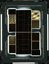
Intel Xe HPC Multi-Chip Module Pictured

Intel SVP for architecture, graphics, and software, Raja Koduri, tweeted the first picture of the Xe HPC scalar compute processor multi-chip module, with its large IHS off. It reveals two large main logic dies built on the 7 nm silicon fabrication process from a third-party foundry. The Xe HPC processor will be targeted at supercomputing and AI-ML applications, so the main logic dies are expected to be large arrays of execution units, spread across what appear to be eight clusters, surrounded by ancillary components such as memory controllers and interconnect PHYs.

There appear to be two kinds of on-package memory on the Xe HPC. The first kind is HBM stacks (from either the HBM2E or HBM3 generation), serving as the main high-speed memory; while the other is a mystery for now. This could either be another class of DRAM, serving a serial processing component on the main logic die; or a non-volatile memory, such as 3D XPoint or NAND flash (likely the former), providing fast persistent storage close to the main logic dies. There appear to be four HBM-class stacks per logic die (so 4096-bit per die and 8192-bit per package), and one die of this secondary memory per logic die.

Micron Also Announces Development of HBMnext

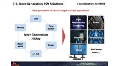
Continuing from the Micron tech brief we shared earlier, a new interesting prospect for the future of ultra-bandwidth solutions is being called simply HBMnext. It's very likely this is only a working title for a next generation HBM memory interface, whether it is a mere evolution of HBM2E or HBM3 proper. The jump in memory speed from HBM2E to HBMnext is still under wraps; however, we've seen HBM2E take significant strides compared to HBM2 already. The first HBM2E products arrived with a 0.4 Gbps improvement over HBM2 (2.4 Gbps vs 2.0 Gbps), but HBM2E has already been certified - and is announced by Micron - as hitting 3.2 Gbps as soon as the second half of this year. One can expect HBMnext to take somewhat comparable strides. Users shouldn't expect to see HBMnext on any products soon, though; it's only expected to launch come 2022.

Samsung Now Mass Producing Industry's First 2nd-Generation 10nm Class DRAM

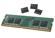
Samsung Electronics Co., Ltd., the world leader in advanced memory technology, announced today that it has begun mass producing the industry's first 2nd-generation of 10-nanometer class (1y-nm), 8-gigabit (Gb) DDR4 DRAM. For use in a wide range of next-generation computing systems, the new 8 Gb DDR4 features the highest performance and energy efficiency for an 8 Gb DRAM chip, as well as the smallest dimensions.

"By developing innovative technologies in DRAM circuit design and process, we have broken through what has been a major barrier for DRAM scalability," said Gyoyoung Jin, president of Memory Business at Samsung Electronics. "Through a rapid ramp-up of the 2nd-generation 10 nm-class DRAM, we will expand our overall 10 nm-class DRAM production more aggressively, in order to accommodate strong market demand and continue to strengthen our business competitiveness."

AMD Navi Found Secretly Hiding in Linux Drivers

We know AMD has been doing a great job keeping the lid on their Navi architecture with information being scarce at the moment. Aside from knowing that Navi is being fabricated on the 7 nm process, it is possible that the microarchitecture will quite possibly support next-generation memory like GDDR6 or HBM3. In a Navi discussion on the Beyond3D forums, a user found an entry in a Linux driver dated back to July that apparently mentions AMD's upcoming architecture - not by its real name, of course. The code is to add support for importing new asic definitions from a text file as opposed to adding support in code. Tom St Denis, a software engineer at AMD, listed the output that would be generated by using this functionality. However, the entry that caught our attention reads: new_chip.gfx10.mmSUPER_SECRET.enable [0: 0]. If our memory serves us right, the codename for Vega was GFX9. So by logic, Navi should carry the GFX10 codename. Obviously, the SUPER_SECRET part further backs up our theory or maybe AMD's just trolling us. The red team has been hiring personnel for their GFX10 projects, so we can assume they're working diligently to release Navi some time next year.

Rambus Talks HBM3, DDR5 in Investor Meeting

Rambus, a company that has veered around the line of being an innovative company and a patent troll, has shed some more light on what can be expected from HBM3 memory (when it's finally available). In an investor meeting, representatives from the company shared details regarding HBM3's improvements over HBM2. Details are still scarce, but at least we know Rambus' expectations for the technology: double the memory bandwidth per stack when compared to HBM2 (4000 MB/s), and a more complex design, which leaves behind the 2.5D design due to increased height of the HBM3 memory stacks. An interesting thing to note is that Rambus is counting on HBM3 to be produced on 7 nm technologies. Considering the overall semiconductor manufacturing calendar for the 7 nm process, this should place HBM3 production in 2019, at the earliest.

HBM3 is also expected to bring much lower power consumption compared to HBM2, besides increasing memory density and bandwidth. However, the "complex design architectures" in the Rambus slides should give readers pause. HBM2 production has had some apparent troubles in reaching demand levels, with suspected lower yields than expected being the most likely culprit. Knowing the trouble AMD has had in successful packaging of HBM2 memory with the silicon interposer and its own GPUs, an even more complex implementation of HBM memory in HBM3 could likely signal some more troubles in that area - maybe not just for AMD, but for any other takers of the technology. Here's hoping AMD's woes were due only to one-off snags on their packaging partners' side, and doesn't spell trouble for HBM's implementation itself.

Samsung Bets on GDDR6 for 2018 Rollout

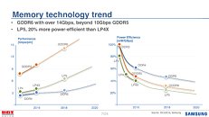
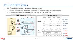
Even as its fellow-Korean DRAM maker SK Hynix is pushing for HBM3 to bring 2 TB/s memory bandwidths to graphics cards, Samsung is betting on relatively inexpensive standards that succeed existing ones. The company hopes to have GDDR6, the memory standard that succeeds GDDR5X, to arrive by 2018.

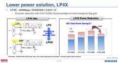
GDDR6 will serve up bandwidths of up to 16 Gbps, up from the 10 Gbps currently offered by GDDR5X. This should enable memory bandwidths of 512 GB/s over a 256-bit wide memory interface, and 768 GB/s over 384-bit. The biggest innovation with GDDR6 that sets it apart from GDDR5X is LP4X, a method with which the memory controller can more responsively keep voltages proportionate to clocks, and reduce power-draw by up to 20% over the previous standard.

Third-Generation HBM Could Enable Graphics Cards with 64GB Memory

One of the first drafts of the HBM3 specification reveals that the standard could enable graphics cards with up to 64 GB of video memory. The HBM2 memory, which is yet to make its consumer graphics debut, caps out at 32 GB, and the first-generation HBM, which released with the AMD Radeon Fury series, at just 4 GB.

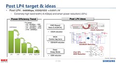
What's more, HBM3 doubles bandwidth over HBM2, pushing up to 512 GB/s per stack. A 4096-bit HBM3 equipped GPU could have up to 2 TB/s (yes, terabytes per second) of memory bandwidth at its disposal. SK Hynix, one of the key proponents of the HBM standard, even claims that HBM3 will be both more energy-efficient and cost-effective than existing memory standards, for the performance on offer. Some of the first HBM3 implementations could come from the HPC industry, with consumer implementations including game consoles, graphics cards, TVs, etc., following later.
Return to Keyword Browsing
Jun 2nd, 2024 07:07 EDT change timezone

New Forum Posts

Popular Reviews

Controversial News Posts