Thursday, January 7th 2010

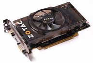
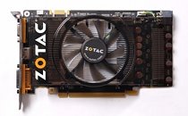
ZOTAC Expands Energy-Efficient Eco Series
"We've had great success with our existing ZOTAC GeForce Eco series graphics cards but many users wanted a higher end model, and thus we engineered the ZOTAC GeForce GTS 250 Eco series," said Carsten Berger, marketing director, ZOTAC International. "Using our experience from the existing ZOTAC GeForce Eco series, we were able to optimize and reduce energy consumption of the award-winning GeForce GTS 250 architecture by a noticeable amount."
Powered by NVIDIA Unified Architecture with 128 unified shaders, the ZOTAC GeForce GTS 250 Eco series deliver compatibility with Microsoft DirectX 10, OpenGL 3.2, NVIDIA PhysX and CUDA enabled games and applications. High-performance DDR3 memory connected via 256-bit memory interface feeds the high-performance graphics processor with maximum energy-efficiency for a visual computing experience that's loaded with stunning realism and performance while maintaining optimal energy-efficiency."With the new ZOTAC GeForce GTS 250 Eco series graphics cards, users can have the best of both worlds - a phenomenal gaming experience that's eco-friendly," Mr. Berger added. It's time to play with the new eco-friendly ZOTAC GeForce GTS 250 Eco.
General Details
- New energy-efficient ZOTAC GeForce GTS 250 Eco series
- Core clock: 675 MHz
- 128 Unified Shaders
- Shader clock: 1620 MHz
- 512MB or 1GB of DDR3 memory
- 256-bit memory interface
- Memory clock: 2000 MHz
- Dual-link DVI output
- HDMI output
- VGA output
- PCI Express 2.0 interface (Compatible with 1.1)
- DirectX 10 with Shader Model 4 compatible
- OpenGL 3.2 compatible
- NVIDIA CUDA & PhysX ready
- NVIDIA PureVideo HD technology


14 Comments on ZOTAC Expands Energy-Efficient Eco Series
8800GT renamed to 9800GT and now GT250 or is it the 8800GTX??. whats next GTX375 ?? please allow it to die. i appreciate your policy "Never say die" lol
Each time it's been renamed the prices have dropped sounds like a win.
Dispite what the price is now on a gts 250 what kind of pricing could you get on an 8800gts + a little overclocking to get relatively the same performance ? To me it just seems like nvidia is falling flat all together on the tech front.
Seriously, if you are giong to troll, at least get the fact straight and make an effort...
Lazy trolls piss me off...1.) The 8800GTS used and extremely weak power setup to make them cheap. The 9800GTX uses a better power setup, talking standard 9800GTX here, not the + version, we'll talk about that later. This mean that the 8800GTS stuggled to even make it to the stock 9800GTX clocks(I know, I had two, neither made it stablely to 9800GTX clocks, one managed to do it on the Core/Shaders, but not the memory).
2.) The 9800GTX+ and GTS250 uses a different core than the 9800GTX and 8800GTS, G92b. This definitely puts the clock speeds way out of 8800GTS range.
3.) The GTS250 is kind of a hybrid, while it retains the G92b core of the 9800GTX+, it uses a PCB that is more like the 8800GTS. Mainly this is a cost saving issue.
The only true renames that we have seen is the 8800GS to 9600GSO, and the 8800GT to 9800GT. And even the 8800GT to 9800GT was originally supposed to be a change, as the 9800GT was supposed to use the 9800GTX PCB, allowing for Tri-SLi(that would have been sweet) and a better power configuration. It was the board partners that basically told nVidia they wouldn't use the new design and were going to continue to use the 8800GT PCB.
By your logic, the HD3870 was just a modified HD2900XT...
You'd be surprised at what some people could achieve on even a 8800GTS 512 with the correct tools.
and not only that Im sure Nvidia had these chips tested at high clock speeds all along. Probably just another way to make more money while spending less money.
[PHP]ATI Radeon™ HD 3800 Series - GPU Specifications
* 666 million transistors on 55nm fabrication process
* PCI Express 2.0 x16 bus interface5
* 256-bit GDDR3/GDDR4 memory interface
* Ring Bus Memory Controller
o Fully distributed design with 512-bit internal ring bus for memory reads and writes
* Microsoft® DirectX® 10.1 support
o Shader Model 4.1[/PHP]
[PHP]ATI Radeon™ HD 2900 Series - GPU Specifications
* 700 million transistors on 80nm HS fabrication process
* 512-bit 8-channel GDDR3/4 memory interface
* Ring Bus Memory Controller
o Fully distributed design with 1024-bit internal ring bus for memory reads and writes
* Microsoft® DirectX® 10 support
o Shader Model 4 [/PHP]
if you are giong to troll, at least get the fact straight and make an effort... 3870 is Dx10.1 and 2900 is Dx10 buddy
I would rather it NOT die and keep competing with ATI's products, or at least until NVIDIA gets the GF100/Fermi-based products out. US$100 (in my area) for this GTS 250 is still very competitive with the ~US$150 HD 5700 series, and is keeping them from going higher.