Thursday, March 4th 2010

GeForce GTX 470 PCB and Cooler Pictured, Too
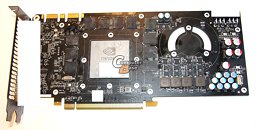
A couple of days after pictures of the PCB and cooling assembly of the GeForce GTX 480 made it to the internet, fresh pictures emerged, this time of the GeForce GTX 470, the slightly toned-down part in the GeForce 400 series. The GTX 470, like the GTX 480, is based on NVIDIA's GF100 core. The reference design PCB is certainly shorter than that of the GTX 480, and compacts its resources. Since the GTX 470 has a 320-bit wide memory interface, it makes do with 10 memory chips, seen surrounding the GPU from three sides. A simpler VRM is used: 4-phase vGPU and 1-phase vMem. Power is drawn in from two 6-pin power connectors.
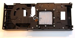
The fan connects over its usual 4-pin PWM-controlled line. Some smart compacting of components made space for two intakes to be cut out, which help the blower draw in some fresh air. The cooling assembly, again is compacted accordingly. Since these new pictures are more clear, we can see that the area over the GPU isn't devoid of a copper surface as earlier thought. In fact, as some community members observed, it is a base with copper heatpipes making direct contact with the GPU. The cooler has protrusions at the right spots to make contact with memory chips and MOSFETs. The GTX 470 is slated to be the more affordable of the GTX 400 series, which will be unveiled on March 26. Follow the source link for equally good quality photography of the GTX 480's PCB.
Source:
ComputerBase.de
The fan connects over its usual 4-pin PWM-controlled line. Some smart compacting of components made space for two intakes to be cut out, which help the blower draw in some fresh air. The cooling assembly, again is compacted accordingly. Since these new pictures are more clear, we can see that the area over the GPU isn't devoid of a copper surface as earlier thought. In fact, as some community members observed, it is a base with copper heatpipes making direct contact with the GPU. The cooler has protrusions at the right spots to make contact with memory chips and MOSFETs. The GTX 470 is slated to be the more affordable of the GTX 400 series, which will be unveiled on March 26. Follow the source link for equally good quality photography of the GTX 480's PCB.


27 Comments on GeForce GTX 470 PCB and Cooler Pictured, Too
Take back my comments in the 480 thread chaps!
:P
GTX 470/480 size comparison:
This definitely gives some good hopes for a simple Dual-GPU card based on these.
The two 6-pins hopefully means that nVidia can put together a dual-GPU card with a single 8-pin and a single 6-pin.
So erreichte bei vierfachem Antialiasing die GeForce GTX 470 durchschnittlich 29 Bilder pro Sekunde (fps), eine Radeon HD 5870 rund 27 fps, die HD 5850 nur 22 fps. Bei achtfachem Antialiasing allerdings bricht die Leistung der GeForce GTX 470 stark ein. Sie erreicht dann nur noch 20 fps, eine Radeon HD 5870 ist bei knapp 23 fps deutlich schneller, die Radeon HD 5850 (19 fps) unterliegt nur knapp.
Running tesselation on a GTX470 - 470 (29fps), 5870 (27fps), 5850 (22fps).
But switching on AA - 470 (20fps), 5870 (23fps), 5850 (19fps).
Yes, thats the 470, not the more powerful 480 but still, thats a 30% performance drop when AA is enabled (compared to a 13-14% drop in the ATI cards). That poly'whatsitcalled' engine isnt looking so hot now.
Right now i am listening to Judas Priest, so these figures must be real.
Single PCB for sure, It'll save money and there isn't really that much stuff to fit in. I'm thinking they could even fit all the memory chips on the front side.
www.techpowerup.com/reviews/Mushkin/GTX_295_Single_PCB/images/front.jpg
www.techpowerup.com/reviews/Mushkin/GTX_295_Single_PCB/images/back.jpg
7 on front and back for each core and that NVIO space could fit the rest 3 chips more needed for double GTX 470. But they could stick 5+5 front and back and use the extra space for cheaper but more space taking VRM part.That. So much speculation going on for months, something real and concrete would be nice. Although seeing the PCBs was nice. These cards can't be that hot with so little stuff. Core maybe, but that isn't hard to cool :)
Considering all the rumors and these picks, someone has to be wrong and I think it is the information about how bad the production issues are. There may be some issues, but it would seem like Nvidia has it well in had now.
It is done to cover the numbers and labels that could be used to trace the card back to person that leaked the pictures. They probably don't want to loose the privilage of having pre-production cards.
Thuough I think it has already been established that they will have two DVI connectors and a mini-HDMI, at least that is what the GTX480 is supposed to have.
Don't really know what was the point of seperate NVIO controller anyways. 8800GT and 9800GTX and rest of the G92 family still gave out picture just fine. Maybe G80 and GT200 was just so big that it was easier to have it seperate? 55nm versions couldn't have it integrated as they were just dieshrinks.
Or seperate NVIO would be better, but they made it integrated to compeate with ATI on price?
And I'm drooling over these just because they would be so easy to cool. They will be way over my budget for a long time, though I have no performance issues either yet :)
It is not a matter of being able to "cramp all the stuff in", but it is a matter of "style" lol.
Can't we just not all stop with the hype - I think it's giving me cancer.
Let's wait not till the 26th but instead till we have some solid reviews. Every 'new' leak of pictures of a card whose performance is in serious doubt is just another batch of Nvidia PR, whether it's sanctioned or not.
Real world reviews = proper graphics news.