Thursday, October 14th 2010

Radeon HD 6870 PCB and GPU Pictured
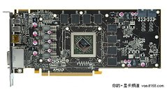
The fine folks at IT168 revealed the first pictures of the Radeon HD 6870 PCB with its cooler completely off, and in its production livery (black). Also let out is the first [clear] picture of the GPU itself. The PCB was first pictured in its nascent qualification sample form, with a development GPU cooler on. The final version of the PCB sticks to its qualification sample for the most part, it has VRM components positioned forwards, trailed by the GPU and its memory. The card makes use of a 4+1+1 phase VRM. All eight memory chips are on the obverse side, each with its own 32-bit wide path, since there's a 256-bit memory interface.
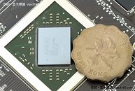
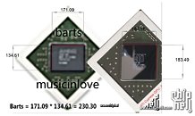
The GPU package is of the same dimensions as the Cypress package, albeit a smaller die. We're getting to hear that Barts is pin-compatible with Cypress (meaning that a Barts GPU can be placed onto a Cypress PCB, given the appropriate BIOS, and it will work), however, no AIB is likely to reuse Cypress PCBs other than for Eyefinity6 designs, because while Barts can make do with a 6-layer PCB, close to every existing Cypress PCB is an 8-layer one, and that Cypress PCBs lack the second mini-DP connector. The die is placed diagonally on the package (à la Cypress and R600), it is rectangular, while the Cypress die is more or less square. ChipHell.com contributor musicinlove did a nice size measurement and comparison. Finally, the AMD "arrow" logo is etched onto the die, it's curtains down for ATI.
Source:
IT168
The GPU package is of the same dimensions as the Cypress package, albeit a smaller die. We're getting to hear that Barts is pin-compatible with Cypress (meaning that a Barts GPU can be placed onto a Cypress PCB, given the appropriate BIOS, and it will work), however, no AIB is likely to reuse Cypress PCBs other than for Eyefinity6 designs, because while Barts can make do with a 6-layer PCB, close to every existing Cypress PCB is an 8-layer one, and that Cypress PCBs lack the second mini-DP connector. The die is placed diagonally on the package (à la Cypress and R600), it is rectangular, while the Cypress die is more or less square. ChipHell.com contributor musicinlove did a nice size measurement and comparison. Finally, the AMD "arrow" logo is etched onto the die, it's curtains down for ATI.


47 Comments on Radeon HD 6870 PCB and GPU Pictured
With the blower style cooler they should see a very nice drop in temps but it greatly depends what the heatsink fo them is like.
Anyway...with the scores these cards are getting. Give them a little while with Driver updates and they will easily beat the 5870/5850.
I doubt there are significant additional performance out of that chip being so small. Remember Nvidia had to use a lot of extra transistors to increase the triangle throughput. Thats why the 460 has a die size similar to the cypress but contains a lot less "cores" 240 vs 320.
Nvidia appears to be the winning combo for dx11 games. ATI for directcompute???
Cayman is what you are looking for. One month to go. :)
like someone else said before, cayman is what you're really waiting for - they are the 6950 and 6970 which will be the real 5870/5850 replacements - should see these towards the end of november.
on top of this there is antilles, the dual gpu solution ( i think dual cayman? ) scheduled for early 2011, but likely to hit around xmas I would expect - this will be the 5970 replacement - likely to be called the 6990 and have some serious powahh!
fun times ahead! :D
This is what I had meant.
It was a rumour with no source to start with and still is.