Thursday, March 8th 2012

AMD Socket FM2 Motherboards Based on A85 FCH Arrive in June
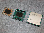
AMD's upcoming A10 and A8 "Trinity" APUs will be built in the new FM2 package for desktop PCs, requiring new motherboards. These APUs will be launched towards the end of Q2, and into Q3 (June-July). A ComputerBase.de report suggests that sources in the motherboard industry it spoke to, at CeBIT, say that socket FM2 motherboards will arrive in June. Further, these motherboards will be based on the new AMD A85 FCH chipset. Not much is known about the A85, except that with the USB-IF certification, it could incorporate native USB 3.0 controllers.
Source:
ComputerBase.de

17 Comments on AMD Socket FM2 Motherboards Based on A85 FCH Arrive in June
Can't wait for benchies, wanna see how the top of the line Lappy 55W APUs as well as the 65W & 100W Desktop ones perform.
Piledriver, new GPU, phew!
Up to 4.2GHz, 384 Radeon Cores 2.0 at 100W TDP
www.fudzilla.com/home/item/25919-amd-trinity-lineup-detailed?tmpl=component&print=1
If you want to crossfire with GCN, then wait for Kaveri which will come with an integrated HD7750.
BTW if I remember correctly someone from AMD said VliW4(5) can be paired with GCN but who knows what impact it has on performance even with comparably strong cards.
These APU are not meant for performance gaming, they are meant for entry and mainstream gaming. The official recommendation is for the dual graphics card to be within a 1-2x performance range of the integrated APU graphics.
All current SI-GCN cards are high performance parts and exceed this guideline. Only a small number of users will be putting large cards in APU systems. This is no different to 68/6900 not being recommended for APU dual graphics.
All Trinity does with whatever GPU they decide to include is raise the bar, it does not redefine the bar.
Eventually the performance CPUs will be updated to maintain the relationship between the mainstream and performance parts.
Some users on the internet think they will be getting a high performance Cayman in Trinity for free just because there has been whispers about what GPU will be included. What architectural it will be doesn't matter as this only affects the effiency.
How they setup whatever GPU is what matters, cores, rop, clockspeed etc
It will be whatever graphics they can fit within to the APU TDP envelope and how much they want to balance CPU v GPU TDP.
Many photos show a larger rectangular trinity die which indicates more emphasis has been put on the GPU but the TDP rules for a desktop still define what they can do, dieshrink and archecture helps but maximum envelopes will never change, the performance achievable within an envelope does however. A mainstream desktop has always been 100W, where as enthusiast can go to 130W safely and workstation 150W. For mobile 45W CPU is seen as the limit?
To complement the headline photo, Here is our own sample of a real Llano die, which gives a better comparison to the relative size of the logic blocks than the press kit die image
www.nitroware.net/images/stories/a6_i3/llano_dieshot.jpg
Versus the press kit supplied image
www.nitroware.net/images/stories/a6_i3/llano_die.jpg
GCN is the architecture that did wonders in performance tests compared to the previous generation even with lower SP counts. I was *really* hoping to see this kind of jump in GPU performance here (to offset pathetic CPU performance) but OTOH it seemed really odd that AMD would jump one generation, given their cautious approach to Llano. Ergo: higly unlikely that Trinirt would have GCN, despite quite some websites suggesting that.
GCN on the other hand is a killer arch with excellent power savings which is right up the APU alley.
Hopefully it makes it in. If it does, it will result in blazing fast integrated graphics, especially when overclocked.
Kaveri (Trinity successor) will be paired with HD7750:)