Sunday, October 6th 2013

NVIDIA Tesla K40 "Atlas" Compute Card Detailed
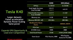
NVIDIA is readying its next big single-GPU compute accelerator, the Tesla K40, codenamed "Atlas." A company slide that's leaked to the web by Chinese publication ByCare reveals its specifications. The card is based on the new GK180 silicon. We've never heard of this one before, but looking at whatever limited specifications that are at hand, it doesn't look too different on paper from the GK110. It features 2,880 CUDA cores.
The card itself offers over 4 TFLOP/s of maximum single-precision floating point performance, with over 1.4 TFLOP/s double-precision. It ships with 12 GB of GDDR5 memory, double that of the Tesla K20X, with a memory bandwidth of 288 GB/s. The card appears to feature a dynamic overclocking feature, which works on ANSYS and AMBER workloads. The chip is configured to take advantage of PCI-Express gen 3.0 system bus. The card will be available in two form-factors, add-on card, and SXM, depending on which the maximum power draw is rated at 235W or 245W, respectively.
Sources:
ByCare, WCCFTech
The card itself offers over 4 TFLOP/s of maximum single-precision floating point performance, with over 1.4 TFLOP/s double-precision. It ships with 12 GB of GDDR5 memory, double that of the Tesla K20X, with a memory bandwidth of 288 GB/s. The card appears to feature a dynamic overclocking feature, which works on ANSYS and AMBER workloads. The chip is configured to take advantage of PCI-Express gen 3.0 system bus. The card will be available in two form-factors, add-on card, and SXM, depending on which the maximum power draw is rated at 235W or 245W, respectively.

25 Comments on NVIDIA Tesla K40 "Atlas" Compute Card Detailed
guys any news about nvidia gtx 800series???realase date or any spec??
This is pure compute - it has no real world consumer benefit to gamers. And you don't need 12Gb memory for 4k. In fact the R9 290X is being touted by AMD as the proper 4k ready card, in other words, 4Gb memory will be more than enough.
help mee :D
In fact, I'm sure if I could summon the mighty W1zzard he'll say why you're very wrong about 8GB for 4K.
let's take bf3 or 4 for example, on ultra, probably going past 1.5gb before any resolution is added to the equation
you can calculate how much space a frame takes up (i forgot... was it 8bit image, 1byte per pixel, 8.3mb for a frame? sounds like i messed up)
by the way, 4k is just 4x1080p, we already do 3x1080p for years with eyefinity/surround, so it's not that massive of a jump (in processing usage)
TPU OSD with GPU Z will give all the info needed in game.
But that means nothing else changes. You are using the same texture maps as the 1080p image. So you can get greater FOV or you get a bigger picture but same quality as 1080p.
If you want to bump up the quality of the picture to UHD+, then you are going to need new texture maps. That means more RAM on the GPU, but also much greater install size of the game. (Bumping up textures 2-4x).
So yes a 2GB 4K card is enough for using legacy 1080 textures, but 8GB for more and UHD texture resources.
It sounds like it makes total sense. In other words, in the future a game like BF5 for 4k resolution texture maps would take upwards of 100GB drive space for all the locations and ultra HD texture maps? Whereas, everything programmed now has a set 'density' of texture and as such at 4k resolution will just be scaled up?
So that makes everybody right!
www.amazon.com/dp/B00BXF7I9M/?tag=tec06d-20
Im waiting for it to come to the UK, but for the price it seems like an affordable 4k setup, they also make a cheaper 39inch version
Lemonsoda says the textures themselves shouldn't take any extra memory even when moving to 4k, and that's true. The frame buffer gets bigger, but that's a paltry 32GB per frame. Even with triple buffering there should be plenty of VRAM to spare. Kinda makes sense, but then there are other things to consider...
If the primitives in a scene become larger dimensionally, then shader operations on those primitives will take up more RAM, no matter that the texture data remains the same size. Each of the stages in the DX11 pipeline has to store data for each primitive, not just the final rendered scene. That means 4x the number of pixels for each triangle, and in a complex scene with lots of triangles that suddenly became bigger, it could easily mean more than 4x the total VRAM required.
Besides, where is the source for your 2015 release date? Don't say Semiaccurate. Other places, just as unprovable say Q1 2014.
So not very interesting to me.
for a start Tmc is Ramping expenditure in 20nm, in laymans terms that means shut up already were on it, i got the stuff on the way and we have it sussed ,honest,, err about yields though.
not shouting about Tsv or 2.5D or cube loud though are they??
If you're expecting daily updates on process fabbing you're shit out of luck since process isn't sexy enough to warrant front page press for mainstream sites- but here's the piece about TSMC's award of BDA's platform partnership, and the design flows for 16nm FinFET (20nm HKMG) to tide you over.