Monday, December 2nd 2013

AMD A10-7850K and A10-7700K APU Specifications Detailed
Specifications of two of AMD's top next-generation APUs, the A10-7850K and A10-7700K, were leaked to the web, revealing an incremental or evolutionary upgrade over the 6000 "Richland" series. To begin with, the two are based on the 28 nm "Kaveri" silicon. Straightaway we find that AMD hasn't been able to catch up with Intel's 22 nm leap for close to two years. All that it manages is to bring the rated TDP of the overclockable "K" chips down to 95W, from the traditional 100W. "Kaveri" puts three of AMD's recent innovations in CPU and GPU on one chip - "Steamroller" CPU micro-architecture, "Graphics CoreNext" GPU architecture, and hUMA (heterogeneous Uniform Memory Access), a technology that allows the CPU and GPU to access the same portion of memory simultaneously.
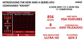
"Steamroller" features the same component hierarchy and basic design as its predecessors "Piledriver" and "Bulldozer," in which clumps of two cores that feature dedicated and shared number-crunching resources, called modules, make up the basic units of a processor. "Kaveri" features two such modules, and hence features four CPU cores. "Kaveri" misses out on an L3 cache cushioning transfers between the modules, and other uncore components on the APU yet again, and each module features a 2-megabyte L2 cache at its last level, totaling the L2 cache amount to 4 MB on "Kaveri." The integrated memory controller features a 128-bit (dual-channel) DDR3 memory interface, with support for standards as high as DDR3-2133 MHz on some models. The PCI-Express root complex complies with the newer PCIe gen 3.0 standard, as do we imagine the A-Link (chipset bus). AMD introduced huge changes with the GPU component.47 percent of the die-area of "Kaveri" is occupied by its GPU, which is designed to restore AMD's competitiveness with Intel's Iris Pro 5000 series. The GPU is based on AMD's "Graphics CoreNext" (GCN) micro-architecture. Physically, there are 512 stream processors present on the chip, arranged in 8 GCN compute units (CUs). Other specifications include 32 TMUs, and 8 ROPs. The GPU supports technologies AMD introduced with its Radeon R7-260X graphics card, including TrueAudio. The GPU supports DirectX 11.2, OpenGL 4.3, and Mantle. It's capable of handling 4K Ultra HD video.
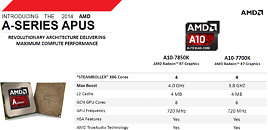
Among the two parts detailed today are the A10-7850K flagship, and the A10-7700K. The A10-7850K features CPU clock speeds of 3.70 GHz, with 4.00 GHz TurboCore frequency, the GPU with all its 512 stream processors unlocked, and GPU clock speeds of 720 MHz. The A10-7700K, on the other hand, offers CPU clock speeds of 3.50 GHz, with 3.80 GHz TurboCore frequencies, and cut-down GPU with just 6 compute units, 384 stream processors, and 24 TMUs clocked at 720 MHz. Both chips are expected to be priced under $150, when they go on sale this January. AMD "Kaveri" APUs are compatible with the newer socket FM2+ motherboards characterized by black-colored CPU sockets, and thicker pins. FM2+ motherboards themselves offer backwards-compatibility with older "Richland" and "Trinity" APUs.
Source:
ProHardware.hu
"Steamroller" features the same component hierarchy and basic design as its predecessors "Piledriver" and "Bulldozer," in which clumps of two cores that feature dedicated and shared number-crunching resources, called modules, make up the basic units of a processor. "Kaveri" features two such modules, and hence features four CPU cores. "Kaveri" misses out on an L3 cache cushioning transfers between the modules, and other uncore components on the APU yet again, and each module features a 2-megabyte L2 cache at its last level, totaling the L2 cache amount to 4 MB on "Kaveri." The integrated memory controller features a 128-bit (dual-channel) DDR3 memory interface, with support for standards as high as DDR3-2133 MHz on some models. The PCI-Express root complex complies with the newer PCIe gen 3.0 standard, as do we imagine the A-Link (chipset bus). AMD introduced huge changes with the GPU component.47 percent of the die-area of "Kaveri" is occupied by its GPU, which is designed to restore AMD's competitiveness with Intel's Iris Pro 5000 series. The GPU is based on AMD's "Graphics CoreNext" (GCN) micro-architecture. Physically, there are 512 stream processors present on the chip, arranged in 8 GCN compute units (CUs). Other specifications include 32 TMUs, and 8 ROPs. The GPU supports technologies AMD introduced with its Radeon R7-260X graphics card, including TrueAudio. The GPU supports DirectX 11.2, OpenGL 4.3, and Mantle. It's capable of handling 4K Ultra HD video.
Among the two parts detailed today are the A10-7850K flagship, and the A10-7700K. The A10-7850K features CPU clock speeds of 3.70 GHz, with 4.00 GHz TurboCore frequency, the GPU with all its 512 stream processors unlocked, and GPU clock speeds of 720 MHz. The A10-7700K, on the other hand, offers CPU clock speeds of 3.50 GHz, with 3.80 GHz TurboCore frequencies, and cut-down GPU with just 6 compute units, 384 stream processors, and 24 TMUs clocked at 720 MHz. Both chips are expected to be priced under $150, when they go on sale this January. AMD "Kaveri" APUs are compatible with the newer socket FM2+ motherboards characterized by black-colored CPU sockets, and thicker pins. FM2+ motherboards themselves offer backwards-compatibility with older "Richland" and "Trinity" APUs.


50 Comments on AMD A10-7850K and A10-7700K APU Specifications Detailed
also, why only ddr3 2133 support? ddr3 2133 is just enough to drive the current models. it wont be enough to feed the new models.
a10 5800k: 8rops, 48TMUS @800mhz
this new a10 7850k only: 8rops, 32TMUS @720
again no L3 cache and only 4mo on L2
...
Nowhere does it say officially what the ROP count will be, but 16 is the leading guesstimate. Also, Trinity/Richland NEVER had 48 TMUs I guess you guys are drunk, since you're seeing double, it had 24, Kaveri has 32. Also V.I. GCN >>> VLIW4.
As for memory support, it isn't all that easy to implement a IMC that is guaranteed to do more than 2133, but just FYI... there's this thing called overclocking(/tweaking) anyway, look it up.
I'll stay just a bit sceptical about this, k...
Look guys. When looking at those APUs you gotta ask yourself:
Who will use those? The ones who will game? The ones who will work?
I think the biggest problem of this APU isn't its GPU part but CPU part.
You see, nowdays when somebody want a good CPU for all uses + HD movies now and then he will buy a core i3 with higher per-core performance.
A gamer who likes some gaming? most chances are that he will buy an i3 or a pentium dual-core + a 80-100$ dedicated graphics card. he will have higher per-core performance and much higher GPU power.
If you're going to have an APU, make it worth your money, at least for some uses. Have an "ok" per-core performance? combine with a serious GPU power for lite-gaming scenarios.
At this time the GPU isn't strong enough for serious 2013 gaming (even at medium settings) but way "too" strong for any other GPU use like movies and 2D indie games.
I see this everyday with costumers.
My 2 cents.
P.S. what have the costumers to do with the thread? ;)
Start by axing the FX 4000. Keep the FX 6000 and FX 8000 (but, work out the per-core thing just a little more and beat intel in cache, pls)(I'm ignoring mantle).
Then, ok, APUs are limited as dual to tetra-threaded CPUs. Add L3 cache. Seriously! And get that iGPU into HD 7670/7750 territory.
I DON'T GIVE A DAMN IF IT'S REDUNDANT!!
Hear me out.
Remember side-port memory?
Find a way to make that exist again. With GDDR5. Because a 7750 with DDR3 is like an Agera with 12'' rims. Idk, make a SO-DIMM with 1GB GDDR5...for 80$, everyone will buy it.
Then, dual-graphics. Three-way-DG possible.
Now here's your marketing pitch:
"Here's a CPU that's not only overkill for an HTPC, but actually passes as a budget gaming machine. For 125~135$. Also, you can add two more HD 7750s (or Rx 2xx rebranded whatever) for more ass haulin'."
There.
P.S.: In case I add a R9 290, the iGPU should still be usable for whatever non-graphical related. Or, at least for things like folding on the side. Since currently, once a non-DG-compatible card is installed, the iGPU goes AWOL. Wasteful.
P.P.S.: Yes, I do live in a dream world.
/RANT
Are Kaveri APU's backwards capable with FM2 boards? Like the A85x FCH?
Seems like a swap with this chip would give a "better" performance boost.
Having used a A8-3850 and A8-3870k I can assure you that these APUs are very capable. Fast DDR3 and the upcoming DDR4 will help alleviate bandwidth problems. Future of DDR4 is very promising. Sideport memory makes no sense from a cost perspective.
I'm glad AMD is focusing on the APU. Once the GPU side is purposed with CPU-compute tasks we'll see an interesting shift in performance.
32nm still allows for a lot and a 125W ceiling isn't something new for AMD parts. Since there's a iGPU in there, it would be understandable.
I know the APUs are very capable, but they also come with some shortcomings, in my opinion. It's those shortcomings that I'd like to see solved.
Sideport vRAM was just something that came to my mind. I didn't really gave much thought about it. But you have to admit that after a certain GPU performance level, DDR3 is a hindrance. And that is noticeable in the 7750.
I'm also eager to see DDR4 hit the market.