Monday, July 11th 2022

NVIDIA PrefixRL Model Designs 25% Smaller Circuits, Making GPUs More Efficient

When designing integrated circuits, engineers aim to produce an efficient design that is easier to manufacture. If they manage to keep the circuit size down, the economics of manufacturing that circuit is also going down. NVIDIA has posted on its technical blog a technique where the company uses an artificial intelligence model called PrefixRL. Using deep reinforcement learning, NVIDIA uses the PrefixRL model to outperform traditional EDA (Electronics Design Automation) tools from major vendors such as Cadence, Synopsys, or Siemens/Mentor. EDA vendors usually implement their in-house AI solution to silicon placement and routing (PnR); however, NVIDIA's PrefixRL solution seems to be doing wonders in the company's workflow.

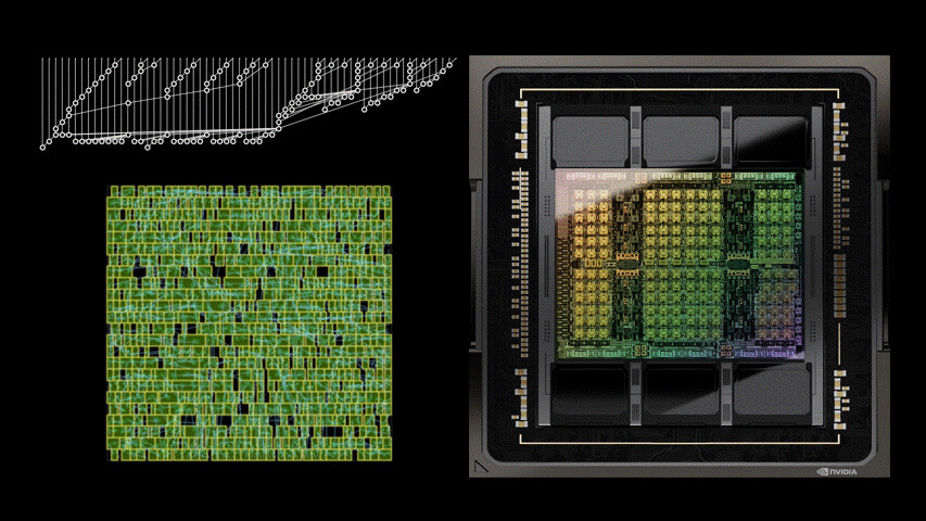
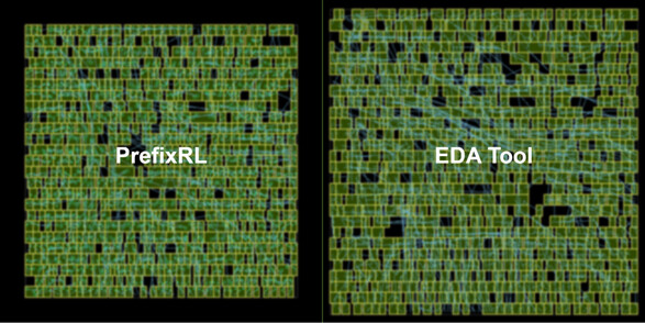
Creating a deep reinforcement learning model that aims to keep the latency the same as the EDA PnR attempt while achieving a smaller die area is the goal of PrefixRL. According to the technical blog, the latest Hopper H100 GPU architecture uses 13,000 instances of arithmetic circuits that the PrefixRL AI model designed. NVIDIA produced a model that outputs a 25% smaller circuit than comparable EDA output. This is all while achieving similar or better latency. Below, you can compare a 64-bit adder design made by PrefixRL and the same design made by an industry-leading EDA tool.
Training such a model is a compute-intensive task. NVIDIA reports that the training to design a 64-bit adder circuit took 256 CPU cores for each GPU and 32,000 GPU hours. The company developed Raptor, an in-house distributed reinforcement learning platform that takes unique advantage of NVIDIA hardware for this kind of industrial reinforcement learning, which you can see below and how it operates. Overall, the system is pretty complex and requires a lot of hardware and input; however, the results pay off with smaller and more efficient GPUs.
Source: NVIDIA
Add your own comment

43 Comments on NVIDIA PrefixRL Model Designs 25% Smaller Circuits, Making GPUs More Efficient

#26
Wirko
They didn't explain exactly what was reduced. Probably a combination of less wasted space between transistors, fewer transistors overall, and fewer large transistors (those that need to be larger because they need to drive larger currents).
Posted on Reply
#27
Punkenjoy
bugBetter than what? It's better than the classic attempts by a measurable 25%. Better than the perfect design? Probably not.
You said Nvidia use a better model from the time being, i just wanted to know why you were saying that. So Better model than a classic attempt? or Better model than other competitors ai model ?
Posted on Reply
#28
bug
PunkenjoyYou said Nvidia use a better model from the time being, i just wanted to know why you were saying that. So Better model than a classic attempt? or Better model than other competitors ai model ?
Well, whatever they use, has to be better, since it yields something smaller than everybody else.
Like @Valantar said, others have not confirmed using AI, so I'm sure there are neural networks or something like that to compare. But the solution overall is clearly better.
Posted on Reply
#31
R0H1T
Of course, it's right there ~
Our method has been used in production to design the next generation of Google TPU,” wrote the authors of the paper, led by Google’s co-heads of machine learning for systems, Azalia Mirhoseini and Anna Goldie.
Posted on Reply
#32
Punkenjoy
bugWell, whatever they use, has to be better, since it yields something smaller than everybody else.
Like @Valantar said, others have not confirmed using AI, so I'm sure there are neural networks or something like that to compare. But the solution overall is clearly better.
Well it yields something better than most common vendor, we don't know exactly what it look like versus what Intel, AMD, Qualcomm, Apple etc. use right now. They probably all their own in house way of doing it.
Posted on Reply
#33
Valantar
R0H1TOf course, it's right there ~
Interesting! Still, that's a much lower volume and smaller scale chip than a large datacenter GPU.
Posted on Reply
#34
Wirko
bugHard to say. At what point does reinforcement learning become "deep"? It's possible others also use reinforcement learning (at least in some aspect), but treat it like a trade secret and don't talk about it. It's also possible Nvidia is the first that made this work.
What I meant to say is that I am pretty certain, in some form or another, others also use some AI techniques in their product pipelines.
Details sure aren't public but everyone is using reinforcement learning, it's not something they would want to hide.
www.forbes.com/sites/karlfreund/2021/08/09/using-ai-to-help-design-chips-has-become-a-thing
Posted on Reply
#35
bug
R0H1TOf course, it's right there ~
Like I said, it's pretty much impossible for computers to figure out simpler things than designing a CPU (www.iaeng.org/publication/IMECS2008/IMECS2008_pp1897-1901.pdf).
Some sort of "AI" has been employed by these problems for decades.

What we should be concentrating on, is what exactly passes as "AI". Years ago, AI was defined as something able to pass the Turing test (en.wikipedia.org/wiki/Turing_test). It needed to learn and adapt. In the past few years, "AI" means a neural network, deeper than 3 or 4 layers (hence deep-everything). It learns nothing once deployed, but it can be trained further and deployed again. And while that may yet qualify as a passable definition of AI (by very, very lax standards), once AI has become a buzzword, now almost every program that an if in it, claims to be employing "AI".
So you see, it's if other have been employing AI, imho, it's determining what they mean by AI when they said they used it.
Posted on Reply
#36
Wirko
bugWhat we should be concentrating on, is what exactly passes as "AI". Years ago, AI was defined as something able to pass the Turing test (en.wikipedia.org/wiki/Turing_test). It needed to learn and adapt. In the past few years, "AI" means a neural network, deeper than 3 or 4 layers (hence deep-everything). It learns nothing once deployed, but it can be trained further and deployed again. And while that may yet qualify as a passable definition of AI (by very, very lax standards), once AI has become a buzzword, now almost every program that an if in it, claims to be employing "AI".
So you see, it's if other have been employing AI, imho, it's determining what they mean by AI when they said they used it.
In lack of a good definition, this one is at least easy to memorise:

Difference between machine learning and AI:
If it is written in Python, it's probably machine learning
If it is written in PowerPoint, it's probably AI
Posted on Reply
#37
Panther_Seraphin
bonehead123And don't forget the most important aspect (for Ngreedia).....

HIGHER PRICES !


Yes I know R&D aint cheap, but this all sounds like just ANUTHA way to justify keeping GPU prices & profits at scalper/pandemic levels, which they have become addicted to like crackheads & their rocks... they always need/want moar and can't quit even if they wanted to....
More like keep current high prices while being able to be reduce costs/decrease die size increasing yields and increasing more dies per wafer.
Posted on Reply
#38
Steevo
I would wager they trained it to look out for standing wave resonance in traces, induction lessening the need for capacitors, harmonic interference from nearby traces or switching speed, gate voltage roll off and all of the fun stuff that usually gets traces moved away from each other to prevent issues at design speed/TDP.

there are formulas for all of this but the actual chip may have required a few spins to get on target and this AI may be able to do it in software and also seems to eliminate the wasted space due to design flaws.
Posted on Reply
#39
R-T-B
ValantarThat's mainly because they're centre aligned. If they were corner aligned instead, the difference would be a lot more intuitive, even if it still doesn't "look like 25% less".
That's also a single adder circuit, not a complete die.
PunkenjoyI know AMD does it, and like you, pretty sure Intel and other manufacturer use AI too. But what make you think Nvidia use a better model ?
The article we just read?
PunkenjoySo Better model than a classic attempt?
There is no "classic attempt." All manufacturers use AI-driven algos to design circuits. This is in the article above.
WirkoDetails sure aren't public but everyone is using reinforcement learning, it's not something they would want to hide.
www.forbes.com/sites/karlfreund/2021/08/09/using-ai-to-help-design-chips-has-become-a-thing
I mean the article literally says this too. My god the arguments we'd save if people read the whole article.
Posted on Reply
#40
Punkenjoy
R-T-BThat's also a single adder circuit, not a complete die.


The article we just read?


There is no "classic attempt." All manufacturers use AI-driven algos to design circuits. This is in the article above.


I mean the article literally says this too. My god the arguments we'd save if people read the whole article.
So the article say Intel, Apple, AMD and others big chip manufacturer use the 2 tools listed in the article ? I don't think so. They could use those, but it's not something declared in the article
Posted on Reply
#41
R-T-B
PunkenjoySo the article say Intel, Apple, AMD and others big chip manufacturer use the 2 tools listed in the article ? I don't think so. They could use those, but it's not something declared in the article
Do you need me to literally quote it for you?
AleksandarKNVIDIA uses the PrefixRL model to outperform traditional EDA (Electronics Design Automation) tools from major vendors such as Cadence, Synopsys, or Siemens/Mentor. EDA vendors usually implement their in-house AI solution to silicon placement and routing (PnR); however, NVIDIA's PrefixRL solution seems to be doing wonders in the company's workflow.
Of course some huge companies may use something different, but this is the industry norm and it's all AI driven.
Posted on Reply
#42
Punkenjoy
R-T-BDo you need me to literally quote it for you?


Of course some huge companies may use something different, but this is the industry norm and it's all AI driven.
Yes, i never said they do not use AI. From what i know, they all declared they do. What i say is about this line:
NVIDIA uses the PrefixRL model to outperform traditional EDA (Electronics Design Automation) tools from major vendors such as Cadence, Synopsys, or Siemens/Mentor. EDA vendors usually implement their in-house AI solution to silicon placement and routing (PnR); however, NVIDIA's PrefixRL solution seems to be doing wonders in the company's workflow.
My point is Nvidia is saying beating these vendors but we do not know how it stack against what other chip maker use. They can/could use their own ai model internally like Nvidia do. So it's nice for Nvidia but it's an incomplete picture and people should remain cautious of the signification of this claim.
Posted on Reply
#43
R0H1T
Well here's the thing, since they're all competing with each other they won't publish like for like results against each other's (AI driven) methods not unless they have a spy & they announce this to the world showing the comparison :D
Posted on Reply
Add your own comment
May 29th, 2024 07:05 EDT change timezone

New Forum Posts

Popular Reviews

Controversial News Posts