Friday, December 12th 2008

AMD Sets RV775 to Chase Down G200b?
Sources tell Expreview that AMD is working on a new graphics processor (apart from the mysterious RV790), as an immediate reaction to the 55nm high-end GPUs NVIDIA is set to release. NVIDIA on its part is working on GeForce GTX 260 (55nm), GeForce GTX 285 (successor to GeForce GTX 280) and the dual-GPU monstrosity, GeForce GTX 295. To rival this, according to the source, AMD is working on the RV775 and derivatives based on its yields' performance.
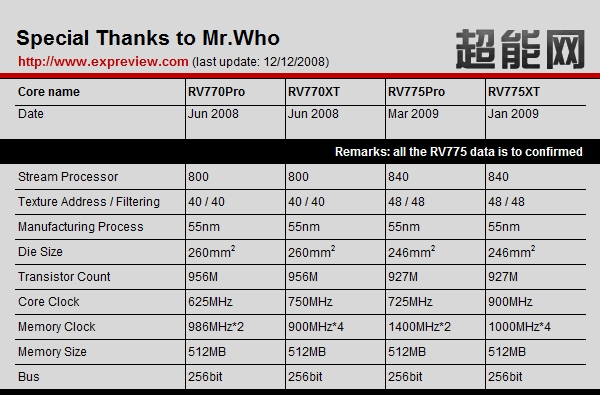
These GPUs are slated for January thru March 2009. It has some very interesting specifications. To begin with, 840 stream processors. While stream processors on a current generation RV770 cannot be added/subtracted in quantities of 40 stream processors, perhaps, the increment of 40 SPs is derived from an extra ALU cluster the RV770 comes with by default (which helps in die harvesting, where the spare ALU cluster makes up for any damaged cluster, thereby improving yields). This would require near-perfect GPUs in the making (if re-engineering of the RV770 on a large scale is to be avoided). Another interesting point is regarding the smaller die. At this point we are clueless as to how that is possible without re-engineering the RV770 at a large scale. Treat yourselves to the specifications meanwhile:
Source:
Expreview
These GPUs are slated for January thru March 2009. It has some very interesting specifications. To begin with, 840 stream processors. While stream processors on a current generation RV770 cannot be added/subtracted in quantities of 40 stream processors, perhaps, the increment of 40 SPs is derived from an extra ALU cluster the RV770 comes with by default (which helps in die harvesting, where the spare ALU cluster makes up for any damaged cluster, thereby improving yields). This would require near-perfect GPUs in the making (if re-engineering of the RV770 on a large scale is to be avoided). Another interesting point is regarding the smaller die. At this point we are clueless as to how that is possible without re-engineering the RV770 at a large scale. Treat yourselves to the specifications meanwhile:
23 Comments on AMD Sets RV775 to Chase Down G200b?
This could be true. Maybe the ripped anything not gaming related and made just a pure gaming card.
Anyway IMO this is false or just some kind of viral marketing to the RV790 or is the RV790 in any case. BUt BOTH won't be released IMO.
RV770 has 956 million transistors according to some sites, and 965 million according to others. Somewhere there is a typo. Let's assume 956 is correct since this is the most popular, then
How would ATI REDUCE the number of transistors whilst INCREASING the number of shaders. What is being changed here? Unless there is another typo and they are increasing the transistor count and going from 55nm to 50 nm. OR they are reducing voltage and increasing the density WITHIN 55nm scale to get the same or more transistors in a smaller space. BUT that is a major tape-out redesign issue.
The table and the technology and the statement no major redesign is mutually inconsistent.
***
What I dont like is that for ATI/AMD shaders are NOT the bottleneck, but TMU and ROPs are: see forums.techpowerup.com/showthread.php?p=1062008.
Therefore meh! They are adding something that doesnt add performance value. :pimp: They are "fixing" the wrong end of the stick.
12 clusters x 14 SP x 5 ALU = 840 SP???
remember last time they where saying 400 sp's or 600 or whatever, and it turned out to be 800, does anyone else make this connection ?
It looks like ATI will do the same thing as they did with the hd3000 series.
with the old r600 it encompases every card from hd2000 series through the hd3000 series,
I got this gut feeling these will get dubbed radeon 4900 series or 4890 or something of that nature.
www.fudzilla.com/index.php?option=com_content&task=view&id=10930&Itemid=1