mAlkAv!An
New Member
- Joined
- May 31, 2011
- Messages
- 2 (0.00/day)
- Location
- Greifswald, Germany
Sapphire HD5850 Xtreme / HD6850 Volt-Mods (vGPU & vMEM)
overview
The PCB is identical to those of HD6850s with AMD reference design. This means these mods can be used for HD6850 as well
A 4-phase switching regulator, which is located between the GPU and output panel, controls the GPU voltage. For the memory a simple single phase switching reg is beeing used.

voltage measurement
output caps of both switching regs are always a good spot for voltage readings. though the little MLCC at the back of VRAM ICs and GPU will give you a more accurate reading.

If u are using software like Trixx to adjust vGPU be aware that those values are different to the real voltage. Here's a table with exact measurement:

*Spannung=voltage
*Last=load
vGPU mod
IC: CHiL 8214
FP Pin: Pin 4 (VSEN)
original resistance: 12.4 Ohms
recommended VR size: 500 Ohms

*Masse = ground
*put a 500 Ohm VR between FB Pin and GND
vMEM mod
IC: APW7165
FP Pin: Pin 6
original resistance: 5010 Ohms
recommended VR size: 200k Ohms
Pin 3 is a good ground spot. A pencil mod is possible alternatively

overclocking
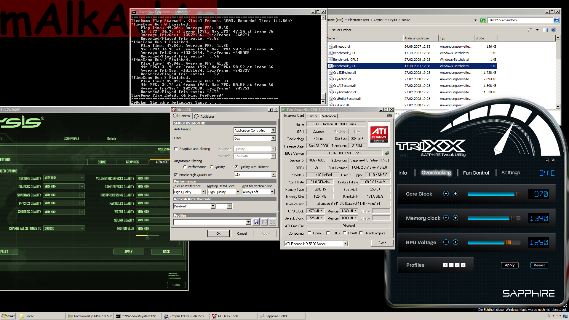
I did some tests with the integrated benchmark of Crysis. Tested in 1920x1080px, DX10 very high details, HQ 16:1 AF and no anti aliasing.
Max. clocks at default voltages are 850MHz(GPU)/1300MHz(VRAM). With an increased GPU voltage of 1.29V(real) and 1.66V VRAM voltage it runs completely stable and without any artifacts at 970/1340MHz. For now I didn't tested more volts because of the stock cooler and high ambient temps.
Benchmarks will run with more than 1000MHz GPU clock.

overview
The PCB is identical to those of HD6850s with AMD reference design. This means these mods can be used for HD6850 as well
A 4-phase switching regulator, which is located between the GPU and output panel, controls the GPU voltage. For the memory a simple single phase switching reg is beeing used.
voltage measurement
output caps of both switching regs are always a good spot for voltage readings. though the little MLCC at the back of VRAM ICs and GPU will give you a more accurate reading.
If u are using software like Trixx to adjust vGPU be aware that those values are different to the real voltage. Here's a table with exact measurement:
*Spannung=voltage
*Last=load
vGPU mod
IC: CHiL 8214
FP Pin: Pin 4 (VSEN)
original resistance: 12.4 Ohms
recommended VR size: 500 Ohms
*Masse = ground
*put a 500 Ohm VR between FB Pin and GND
vMEM mod
IC: APW7165
FP Pin: Pin 6
original resistance: 5010 Ohms
recommended VR size: 200k Ohms
Pin 3 is a good ground spot. A pencil mod is possible alternatively
overclocking
I did some tests with the integrated benchmark of Crysis. Tested in 1920x1080px, DX10 very high details, HQ 16:1 AF and no anti aliasing.
Max. clocks at default voltages are 850MHz(GPU)/1300MHz(VRAM). With an increased GPU voltage of 1.29V(real) and 1.66V VRAM voltage it runs completely stable and without any artifacts at 970/1340MHz. For now I didn't tested more volts because of the stock cooler and high ambient temps.
Benchmarks will run with more than 1000MHz GPU clock.