Report an Error


NVIDIA GeForce 8600 GT
- Graphics Processor
- G84
- Cores
- 32
- TMUs
- 16
- ROPs
- 8
- Memory Size
- 512 MB
- Memory Type
- GDDR3
- Bus Width
- 128 bit

GPU
Recommended Gaming Resolutions:
- 640x480
- 1280x720
- 1366x768
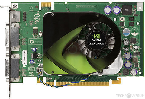
The GeForce 8600 GT was a mid-range graphics card by NVIDIA, launched on April 17th, 2007. Built on the 80 nm process, and based on the G84 graphics processor, in its G84-303-A2 variant, the card supports DirectX 11.1. Even though it supports DirectX 11, the feature level is only 10_0, which can be problematic with many DirectX 11 & DirectX 12 titles. The G84 graphics processor is an average sized chip with a die area of 169 mm² and 289 million transistors. It features 32 shading units, 16 texture mapping units, and 8 ROPs. NVIDIA has paired 512 MB GDDR3 memory with the GeForce 8600 GT, which are connected using a 128-bit memory interface. The GPU is operating at a frequency of 540 MHz, memory is running at 700 MHz.
Being a single-slot card, the NVIDIA GeForce 8600 GT does not require any additional power connector, its power draw is rated at 47 W maximum. Display outputs include: 2x DVI, 1x S-Video. GeForce 8600 GT is connected to the rest of the system using a PCI-Express 1.0 x16 interface. The card measures 170 mm in length, and features a single-slot cooling solution. Its price at launch was 159 US Dollars.
Being a single-slot card, the NVIDIA GeForce 8600 GT does not require any additional power connector, its power draw is rated at 47 W maximum. Display outputs include: 2x DVI, 1x S-Video. GeForce 8600 GT is connected to the rest of the system using a PCI-Express 1.0 x16 interface. The card measures 170 mm in length, and features a single-slot cooling solution. Its price at launch was 159 US Dollars.
Graphics Processor
Graphics Card
- Release Date
- Apr 17th, 2007
- Generation
-
GeForce 8
(8600)
- Predecessor
- GeForce 7 PCIe
- Successor
- GeForce 9
- Production
- End-of-life
- Launch Price
- 159 USD
- Bus Interface
- PCIe 1.0 x16
- Reviews
- 183 in our database
Relative Performance
Based on TPU review data: "Performance Summary" at 1920x1080, 4K for 2080 Ti and faster.
Performance estimated based on architecture, shader count and clocks.
Clock Speeds
- GPU Clock
- 540 MHz
- Shader Clock
- 1190 MHz
- Memory Clock
-
700 MHz
1400 Mbps effective
Memory
- Memory Size
- 512 MB
- Memory Type
- GDDR3
- Memory Bus
- 128 bit
- Bandwidth
- 22.40 GB/s
Render Config
- Shading Units
- 32
- TMUs
- 16
- ROPs
- 8
- SM Count
- 4
- L2 Cache
- 32 KB
Theoretical Performance
- Pixel Rate
- 4.320 GPixel/s
- Texture Rate
- 8.640 GTexel/s
- FP32 (float)
- 76.16 GFLOPS
Board Design
- Slot Width
- Single-slot
- Length
- 170 mm
6.7 inches
- TDP
- 47 W
- Suggested PSU
- 200 W
- Outputs
- 2x DVI
1x S-Video
- Power Connectors
- None
- Board Number
- P402,
P403 SKU 6
Graphics Features
- DirectX
- 11.1 (10_0)
- OpenGL
- 3.3
- OpenCL
- 1.1
- Vulkan
- N/A
- CUDA
- 1.1
- Shader Model
- 4.0
Card Notes
| Memory Variant: 1 GB |
G84 GPU Notes
| PureVideo HD: VP2 VDPAU: Feature Set A Latest Drivers: Windows 2000: Quadro Release 261.19 Windows XP / Server 2003 x64: GeForce Release 185.81 (Notebooks) GeForce Release 340.52 Quadro Release R319 U2 (321.01) Tesla Release 258.96 Windows Vista: GeForce Release 307.83 (Notebooks) GeForce Release 342.01 Quadro Release R340 U15 (342.01) Tesla Release 258.96 Windows 7 / 8 / 8.1 / 10: GeForce Release 342.01 Quadro Release R340 U15 (342.01) Tesla Release 258.96 |
Retail boards based on this design (4)
| Name | GPU Clock | Memory Clock | Other Changes |
|---|---|---|---|
| 540 MHz | 800 MHz | DDR2, 1x DVI 1x VGA 1x S-Video | |
| 540 MHz | 700 MHz | 256 MB | |
| 620 MHz | 800 MHz | 256 MB | |
| 600 MHz | 800 MHz | 161 mm/6.3 inches |


Mar 24th, 2025 21:22 EDT
change timezone
Latest GPU Drivers
New Forum Posts
- RTX 5080 locked at 750 MHZ in certain games (15)
- Your PC ATM (35287)
- Last game you purchased? (745)
- Help with Nginx Reverse Proxy (6)
- RTX 5080 worth it over 5070 TI for 4k? (36)
- What's your latest tech purchase? (23382)
- HalfLife2 RTX Demo Is out! (294)
- Postulation: Is anyone else concerned with the proliferation of AI? (303)
- Windows 10 Vs 11, Which one too choose? (75)
- Is RX 9070 VRAM temperature regular value or hotspot? (174)
Popular Reviews
- Assassin's Creed Shadows Performance Benchmark Review - 30 GPUs Compared
- ASUS ProArt X870E-Creator Wi-Fi Review
- ASRock Radeon RX 9070 XT Taichi OC Review - Excellent Cooling
- Sapphire Radeon RX 9070 XT Nitro+ Review - Beating NVIDIA
- ASUS GeForce RTX 5070 TUF OC Review
- be quiet! Pure Rock Pro 3 Black Review
- AMD Ryzen 9 9950X3D Review - Great for Gaming and Productivity
- Quick Look: Jelly Key Mystic Snake Artisan Keycaps
- AMD Ryzen 7 9800X3D Review - The Best Gaming Processor
- ASUS Radeon RX 9070 TUF OC Review
Controversial News Posts
- NVIDIA GeForce RTX 50 Cards Spotted with Missing ROPs, NVIDIA Confirms the Issue, Multiple Vendors Affected (519)
- AMD RDNA 4 and Radeon RX 9070 Series Unveiled: $549 & $599 (260)
- AMD Mentions Sub-$700 Pricing for Radeon RX 9070 GPU Series, Looks Like NV Minus $50 Again (250)
- AMD Radeon RX 9070-series Pricing Leaks Courtesy of MicroCenter (158)
- MSI Doesn't Plan Radeon RX 9000 Series GPUs, Skips AMD RDNA 4 Generation Entirely (142)
- Microsoft Introduces Copilot for Gaming (123)
- AMD Radeon RX 9070 XT Reportedly Outperforms RTX 5080 Through Undervolting (118)
- NVIDIA Reportedly Prepares GeForce RTX 5060 and RTX 5060 Ti Unveil Tomorrow (115)