Report an Error


NVIDIA GeForce 8400 GS Rev. 3
- Graphics Processor
- GT218S
- Cores
- 8
- TMUs
- 4
- ROPs
- 4
- Memory Size
- 512 MB
- Memory Type
- DDR2
- Bus Width
- 64 bit

GPU
Recommended Gaming Resolutions:
- 640x480
- 1280x720
- 1366x768
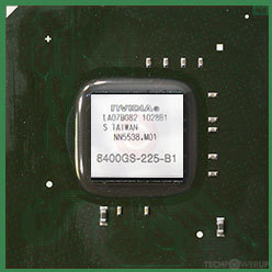
The GeForce 8400 GS Rev. 3 was a graphics card by NVIDIA, launched on July 12th, 2010. Built on the 40 nm process, and based on the GT218S graphics processor, in its 8400GS-225-B1 variant, the card supports DirectX 11.1. Even though it supports DirectX 11, the feature level is only 10_1, which can be problematic with many DirectX 11 & DirectX 12 titles. The GT218S graphics processor is a relatively small chip with a die area of only 57 mm² and 260 million transistors. Unlike the fully unlocked GeForce 8400 GS PCI Rev. 2, which uses the same GPU but has all 16 shaders enabled, NVIDIA has disabled some shading units on the GeForce 8400 GS Rev. 3 to reach the product's target shader count. It features 8 shading units, 4 texture mapping units, and 4 ROPs. NVIDIA has paired 512 MB DDR2 memory with the GeForce 8400 GS Rev. 3, which are connected using a 64-bit memory interface. The GPU is operating at a frequency of 520 MHz, memory is running at 400 MHz.
Being a single-slot card, the NVIDIA GeForce 8400 GS Rev. 3 does not require any additional power connector, its power draw is rated at 25 W maximum. Display outputs include: 1x DVI, 1x VGA, 1x S-Video. GeForce 8400 GS Rev. 3 is connected to the rest of the system using a PCI-Express 2.0 x16 interface. The card measures 170 mm in length, and features a single-slot cooling solution.
Being a single-slot card, the NVIDIA GeForce 8400 GS Rev. 3 does not require any additional power connector, its power draw is rated at 25 W maximum. Display outputs include: 1x DVI, 1x VGA, 1x S-Video. GeForce 8400 GS Rev. 3 is connected to the rest of the system using a PCI-Express 2.0 x16 interface. The card measures 170 mm in length, and features a single-slot cooling solution.
Graphics Processor
Graphics Card
- Release Date
- Jul 12th, 2010
- Generation
-
GeForce 8
(8400)
- Predecessor
- GeForce 7 PCIe
- Successor
- GeForce 9
- Production
- End-of-life
- Bus Interface
- PCIe 2.0 x16
- Reviews
- 10 in our database
Relative Performance
Based on TPU review data: "Performance Summary" at 1920x1080, 4K for 2080 Ti and faster.
Performance estimated based on architecture, shader count and clocks.
Clock Speeds
- GPU Clock
- 520 MHz
- Shader Clock
- 1230 MHz
- Memory Clock
-
400 MHz
800 Mbps effective
Memory
- Memory Size
- 512 MB
- Memory Type
- DDR2
- Memory Bus
- 64 bit
- Bandwidth
- 6.400 GB/s
Render Config
- Shading Units
- 8
- TMUs
- 4
- ROPs
- 4
- SM Count
- 1
- L2 Cache
- 32 KB
Theoretical Performance
- Pixel Rate
- 2.080 GPixel/s
- Texture Rate
- 2.080 GTexel/s
- FP32 (float)
- 19.68 GFLOPS
Board Design
- Slot Width
- Single-slot
- Length
- 170 mm
6.7 inches
- TDP
- 25 W
- Suggested PSU
- 200 W
- Outputs
- 1x DVI
1x VGA
1x S-Video
- Power Connectors
- None
- Board Number
- P691,
P872 SKU 0,
P872 SKU 2,
P873 SKU 0,
P874 SKU 5
Graphics Features
- DirectX
- 11.1 (10_1)
- OpenGL
- 3.3
- OpenCL
- 1.1
- Vulkan
- N/A
- CUDA
- 1.2
- Shader Model
- 4.1
GT218S GPU Notes
| PureVideo HD: VP4 VDPAU: Feature Set C Latest Drivers: Windows 2000: Quadro Release 261.19 Windows XP / Server 2003 x64: GeForce Release 185.81 (Notebooks) GeForce Release 340.52 Quadro Release R319 U2 (321.01) Tesla Release 258.96 Windows Vista: GeForce Release 307.83 (Notebooks) GeForce Release 342.01 Quadro Release R340 U15 (342.01) Tesla Release 258.96 Windows 7 / 8 / 8.1 / 10: GeForce Release 342.01 Quadro Release R340 U15 (342.01) Tesla Release 258.96 |
Retail boards based on this design (1)
| Name | GPU Clock | Memory Clock | Other Changes |
|---|---|---|---|
| 520 MHz | 600 MHz | 1024 MB, DDR3, 165 mm/6.5 inches, 1x DVI 1x HDMI 1x VGA |

Apr 11th, 2025 00:36 EDT
change timezone
Latest GPU Drivers
New Forum Posts
- What are you playing? (23363)
- (Some of) What I'd like to See From a Final Fantasy IX Remake (14)
- Game Soundtracks You Love (1034)
- Free Games Thread (4614)
- Can the display output be enabled by modifying the vBIOS of the Radeon Pro V620? (5)
- [REQUEST] How to use ThrottleStop to overclock 1630v3 to 4.5ghz on a t5810 workstation? (0)
- Will I benefit from changing the thermal pad? (64)
- Lossless scaling (4)
- I tried to use AMD Auto Overclock, and now my PC has been freezing up sometimes. Afterwards, the screen goes black or displays artifacts. (17)
- The TPU UK Clubhouse (26077)
Popular Reviews
- The Last Of Us Part 2 Performance Benchmark Review - 30 GPUs Compared
- ASRock Z890 Taichi OCF Review
- Thermaltake TR100 Review
- Zotac GeForce RTX 5070 Ti Amp Extreme Review
- Sapphire Radeon RX 9070 XT Pulse Review
- Acer Predator GM9000 2 TB Review
- Sapphire Radeon RX 9070 XT Nitro+ Review - Beating NVIDIA
- Upcoming Hardware Launches 2025 (Updated Apr 2025)
- PowerColor Radeon RX 9070 Hellhound Review
- MCHOSE L7 Pro Review
Controversial News Posts
- NVIDIA GeForce RTX 5060 Ti 16 GB SKU Likely Launching at $499, According to Supply Chain Leak (175)
- MSI Doesn't Plan Radeon RX 9000 Series GPUs, Skips AMD RDNA 4 Generation Entirely (146)
- Microsoft Introduces Copilot for Gaming (124)
- AMD Radeon RX 9070 XT Reportedly Outperforms RTX 5080 Through Undervolting (119)
- NVIDIA Reportedly Prepares GeForce RTX 5060 and RTX 5060 Ti Unveil Tomorrow (115)
- NVIDIA Sends MSRP Numbers to Partners: GeForce RTX 5060 Ti 8 GB at $379, RTX 5060 Ti 16 GB at $429 (104)
- Nintendo Confirms That Switch 2 Joy-Cons Will Not Utilize Hall Effect Stick Technology (103)
- Over 200,000 Sold Radeon RX 9070 and RX 9070 XT GPUs? AMD Says No Number was Given (100)