Report an Error


NVIDIA GeForce 9800 GTX
- Graphics Processor
- G92
- Cores
- 128
- TMUs
- 64
- ROPs
- 16
- Memory Size
- 512 MB
- Memory Type
- GDDR3
- Bus Width
- 256 bit


GPU
I/O
Back
Recommended Gaming Resolutions:
- 1366x768
- 1600x900
- 1920x1080
The GeForce 9800 GTX was a performance-segment graphics card by NVIDIA, launched on March 28th, 2008. Built on the 65 nm process, and based on the G92 graphics processor, in its G92-420-A2 variant, the card supports DirectX 11.1. Even though it supports DirectX 11, the feature level is only 10_0, which can be problematic with many DirectX 11 & DirectX 12 titles. The G92 graphics processor is a large chip with a die area of 324 mm² and 754 million transistors. It features 128 shading units, 64 texture mapping units, and 16 ROPs. NVIDIA has paired 512 MB GDDR3 memory with the GeForce 9800 GTX, which are connected using a 256-bit memory interface. The GPU is operating at a frequency of 675 MHz, memory is running at 1100 MHz.
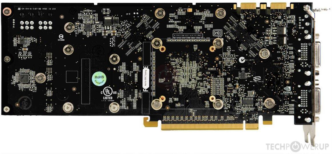
Being a dual-slot card, the NVIDIA GeForce 9800 GTX draws power from 2x 6-pin power connectors, with power draw rated at 140 W maximum. Display outputs include: 2x DVI, 1x S-Video. GeForce 9800 GTX is connected to the rest of the system using a PCI-Express 2.0 x16 interface. The card's dimensions are 267 mm x 111 mm x 38 mm, and it features a dual-slot cooling solution. Its price at launch was 299 US Dollars.
Being a dual-slot card, the NVIDIA GeForce 9800 GTX draws power from 2x 6-pin power connectors, with power draw rated at 140 W maximum. Display outputs include: 2x DVI, 1x S-Video. GeForce 9800 GTX is connected to the rest of the system using a PCI-Express 2.0 x16 interface. The card's dimensions are 267 mm x 111 mm x 38 mm, and it features a dual-slot cooling solution. Its price at launch was 299 US Dollars.
Graphics Processor
Graphics Card
- Release Date
- Mar 28th, 2008
- Generation
-
GeForce 9
(9800)
- Predecessor
- GeForce 8
- Successor
- GeForce 200
- Production
- End-of-life
- Launch Price
- 299 USD
- Bus Interface
- PCIe 2.0 x16
- Reviews
- 84 in our database
Relative Performance
Based on TPU review data: "Performance Summary" at 1920x1080, 4K for 2080 Ti and faster.
Performance estimated based on architecture, shader count and clocks.
Clock Speeds
- GPU Clock
- 675 MHz
- Shader Clock
- 1688 MHz
- Memory Clock
-
1100 MHz
2.2 Gbps effective
Memory
- Memory Size
- 512 MB
- Memory Type
- GDDR3
- Memory Bus
- 256 bit
- Bandwidth
- 70.40 GB/s
Render Config
- Shading Units
- 128
- TMUs
- 64
- ROPs
- 16
- SM Count
- 16
- L2 Cache
- 64 KB
Theoretical Performance
- Pixel Rate
- 10.80 GPixel/s
- Texture Rate
- 43.20 GTexel/s
- FP32 (float)
- 432.1 GFLOPS
Board Design
- Slot Width
- Dual-slot
- Length
- 267 mm
10.5 inches
- Width
- 111 mm
4.4 inches
- Height
- 38 mm
1.5 inches
- TDP
- 140 W
- Suggested PSU
- 300 W
- Outputs
- 2x DVI
1x S-Video
- Power Connectors
- 2x 6-pin
- Board Number
- P392 SKU 1
Graphics Features
- DirectX
- 11.1 (10_0)
- OpenGL
- 3.3
- OpenCL
- 1.1
- Vulkan
- N/A
- CUDA
- 1.1
- Shader Model
- 4.0
G92 GPU Notes
| PureVideo HD: VP2 VDPAU: Feature Set A Latest Drivers: Windows 2000: Quadro Release 261.19 Windows XP / Server 2003 x64: GeForce Release 185.81 (Notebooks) GeForce Release 340.52 Quadro Release R319 U2 (321.01) Tesla Release 258.96 Windows Vista: GeForce Release 307.83 (Notebooks) GeForce Release 342.01 Quadro Release R340 U15 (342.01) Tesla Release 258.96 Windows 7 / 8 / 8.1 / 10: GeForce Release 342.01 Quadro Release R340 U15 (342.01) Tesla Release 258.96 |
Retail boards based on this design (3)
| Name | GPU Clock | Memory Clock | Other Changes |
|---|---|---|---|
| 755 MHz | 1175 MHz | ||
| 675 MHz | 1100 MHz | ||
| 756 MHz | 1150 MHz |


Mar 14th, 2025 21:47 EDT
change timezone
Latest GPU Drivers
New Forum Posts
- The TPU UK Clubhouse (25893)
- Silent Hill Series Discussion/Speculation thread (10)
- Recommended PhysX card for 5xxx series? [Is vRAM relevant?] (145)
- PCI 4.0 16x slot reported as a PCI 5.0 8x with the AMD 9070 XT Reaper GPU (2)
- Fps Drop Problem ??? (9)
- RX 9000 series GPU Owners Club (75)
- i7-9750H laptop overclocking/optimization Question (9)
- So my neighbor bought a new keyboard... (10)
- I7 9750h Thermal Throttling and Power Limit Issue (1)
- New help flashing my GTX 970 I just bought 04G-P4-2978-KR (1)
Popular Reviews
- AMD Ryzen 9 9950X3D Review - Great for Gaming and Productivity
- Sapphire Radeon RX 9070 XT Nitro+ Review - Beating NVIDIA
- Gigabyte X870E Aorus Pro Review
- FSP MP7 Black Review
- XFX Radeon RX 9070 XT Mercury OC Magnetic Air Review
- ASUS GeForce RTX 5090 TUF Review
- ASUS Radeon RX 9070 TUF OC Review
- MSI GeForce RTX 5070 Gaming Trio OC Review
- Dough Spectrum Black 32 Review
- AMD Ryzen 7 9800X3D Review - The Best Gaming Processor
Controversial News Posts
- NVIDIA GeForce RTX 50 Cards Spotted with Missing ROPs, NVIDIA Confirms the Issue, Multiple Vendors Affected (513)
- AMD Radeon RX 9070 and 9070 XT Listed On Amazon - One Buyer Snags a Unit (261)
- AMD RDNA 4 and Radeon RX 9070 Series Unveiled: $549 & $599 (260)
- AMD Mentions Sub-$700 Pricing for Radeon RX 9070 GPU Series, Looks Like NV Minus $50 Again (249)
- NVIDIA Investigates GeForce RTX 50 Series "Blackwell" Black Screen and BSOD Issues (244)
- AMD Radeon RX 9070 and 9070 XT Official Performance Metrics Leaked, +42% 4K Performance Over Radeon RX 7900 GRE (195)
- AMD Radeon RX 9070-series Pricing Leaks Courtesy of MicroCenter (158)
- AMD Radeon RX 9070 XT Reportedly Outperforms RTX 5080 Through Undervolting (113)