Report an Error


NVIDIA GeForce 9600 GSO
- Graphics Processor
- G92
- Cores
- 96
- TMUs
- 48
- ROPs
- 12
- Memory Size
- 384 MB
- Memory Type
- GDDR3
- Bus Width
- 192 bit

GPU
Recommended Gaming Resolutions:
- 1280x720
- 1366x768
- 1600x900
The GeForce 9600 GSO was a graphics card by NVIDIA, launched on April 28th, 2008. Built on the 65 nm process, and based on the G92 graphics processor, the card supports DirectX 11.1. Even though it supports DirectX 11, the feature level is only 10_0, which can be problematic with many DirectX 11 & DirectX 12 titles. The G92 graphics processor is a large chip with a die area of 324 mm² and 754 million transistors. Unlike the fully unlocked GeForce 8800 GTS 512, which uses the same GPU but has all 128 shaders enabled, NVIDIA has disabled some shading units on the GeForce 9600 GSO to reach the product's target shader count. It features 96 shading units, 48 texture mapping units, and 12 ROPs. NVIDIA has paired 384 MB GDDR3 memory with the GeForce 9600 GSO, which are connected using a 192-bit memory interface. The GPU is operating at a frequency of 550 MHz, memory is running at 800 MHz.
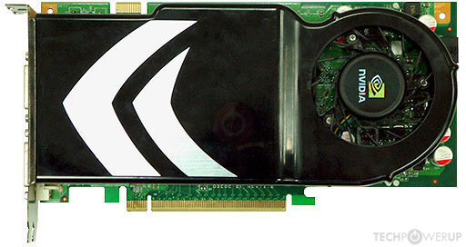
Being a dual-slot card, the NVIDIA GeForce 9600 GSO draws power from 1x 6-pin power connector, with power draw rated at 84 W maximum. Display outputs include: 2x DVI, 1x S-Video. GeForce 9600 GSO is connected to the rest of the system using a PCI-Express 2.0 x16 interface. The card measures 229 mm in length, and features a dual-slot cooling solution.
Being a dual-slot card, the NVIDIA GeForce 9600 GSO draws power from 1x 6-pin power connector, with power draw rated at 84 W maximum. Display outputs include: 2x DVI, 1x S-Video. GeForce 9600 GSO is connected to the rest of the system using a PCI-Express 2.0 x16 interface. The card measures 229 mm in length, and features a dual-slot cooling solution.
Graphics Processor
Graphics Card
- Release Date
- Apr 28th, 2008
- Generation
-
GeForce 9
(9600)
- Predecessor
- GeForce 8
- Successor
- GeForce 200
- Production
- End-of-life
- Bus Interface
- PCIe 2.0 x16
- Reviews
- 4 in our database
Relative Performance
Based on TPU review data: "Performance Summary" at 1920x1080, 4K for 2080 Ti and faster.
Performance estimated based on architecture, shader count and clocks.
Clock Speeds
- GPU Clock
- 550 MHz
- Shader Clock
- 1375 MHz
- Memory Clock
-
800 MHz
1600 Mbps effective
Memory
- Memory Size
- 384 MB
- Memory Type
- GDDR3
- Memory Bus
- 192 bit
- Bandwidth
- 38.40 GB/s
Render Config
- Shading Units
- 96
- TMUs
- 48
- ROPs
- 12
- SM Count
- 12
- L2 Cache
- 48 KB
Theoretical Performance
- Pixel Rate
- 6.600 GPixel/s
- Texture Rate
- 26.40 GTexel/s
- FP32 (float)
- 264.0 GFLOPS
Board Design
- Slot Width
- Dual-slot
- Length
- 229 mm
9 inches
- TDP
- 84 W
- Suggested PSU
- 250 W
- Outputs
- 2x DVI
1x S-Video
- Power Connectors
- 1x 6-pin
- Board Number
- P393 SKU 4,
P393 SKU 12,
P393 SKU 14
Graphics Features
- DirectX
- 11.1 (10_0)
- OpenGL
- 3.3
- OpenCL
- 1.1
- Vulkan
- N/A
- CUDA
- 1.1
- Shader Model
- 4.0
Card Notes
| Variant Memory: 768 MB Variant Memory: 1536 MB |
G92 GPU Notes
| PureVideo HD: VP2 VDPAU: Feature Set A Latest Drivers: Windows 2000: Quadro Release 261.19 Windows XP / Server 2003 x64: GeForce Release 185.81 (Notebooks) GeForce Release 340.52 Quadro Release R319 U2 (321.01) Tesla Release 258.96 Windows Vista: GeForce Release 307.83 (Notebooks) GeForce Release 342.01 Quadro Release R340 U15 (342.01) Tesla Release 258.96 Windows 7 / 8 / 8.1 / 10: GeForce Release 342.01 Quadro Release R340 U15 (342.01) Tesla Release 258.96 |
Retail boards based on this design (5)
| Name | GPU Clock | Memory Clock | Other Changes |
|---|---|---|---|
| 550 MHz | 505 MHz | 512 MB, DDR2, 128 bit | |
| 600 MHz | 900 MHz | ||
| 680 MHz | 900 MHz | ||
| 600 MHz | 900 MHz | 768 MB | |
| 580 MHz | 500 MHz | 768 MB, DDR2, Single-slot |


Feb 3rd, 2025 06:01 EST
change timezone
Latest GPU Drivers
New Forum Posts
- Gigabyte B550 Aorus Elite V2 Default RGB LED (10)
- Will you buy a RTX 5090? (374)
- Choosing the Perfect Motherboard to Complete My PC Build (1)
- Wow YouTube is a Hog (24)
- Trying to install OS and stick to it for 2 Years Atleast. Windows 10 or 11? (12)
- RTX 5080 - premature review - it sucks (278)
- GPU hotspot and Gpu tem differences (9)
- [GUIDE] Unlock the EC TDP limit of your low power U series Intel CPU (21)
- is it possible to enable 105w ECO MODE this way? (2)
- RTX 5090 ridiculous price! (138)
Popular Reviews
- NVIDIA GeForce RTX 5080 Founders Edition Review
- Spider-Man 2 Performance Benchmark Review - 35 GPUs Tested
- MSI GeForce RTX 5080 Vanguard SOC Review
- ASUS GeForce RTX 5080 Astral OC Review
- Gigabyte GeForce RTX 5080 Gaming OC Review
- MSI GeForce RTX 5080 Suprim SOC Review
- NVIDIA DLSS 4 Transformer Review - Better Image Quality for Everyone
- ASUS GeForce RTX 5090 Astral OC Review - Astronomical Premium
- Galax GeForce RTX 5080 1-Click OC Review
- Palit GeForce RTX 5080 GameRock OC Review
Controversial News Posts
- NVIDIA 2025 International CES Keynote: Liveblog (470)
- AMD Debuts Radeon RX 9070 XT and RX 9070 Powered by RDNA 4, and FSR 4 (349)
- AMD Radeon 9070 XT Rumored to Outpace RTX 5070 Ti by Almost 15% (259)
- AMD is Taking Time with Radeon RX 9000 to Optimize Software and FSR 4 (256)
- AMD Denies Radeon RX 9070 XT $899 USD Starting Price Point Rumors (239)
- AMD Radeon RX 9070 XT & RX 9070 Custom Models In Stock at European Stores (226)
- Edward Snowden Lashes Out at NVIDIA Over GeForce RTX 50 Pricing And Value (218)
- New Leak Reveals NVIDIA RTX 5080 Is Slower Than RTX 4090 (215)