Report an Error
NVIDIA GeForce GT 740M
- Graphics Processor
- GK107
- Cores
- 384
- TMUs
- 32
- ROPs
- 16
- Memory Size
- 2 GB
- Memory Type
- DDR3
- Bus Width
- 128 bit
Recommended Gaming Resolutions:
- 1366x768
- 1600x900
- 1920x1080
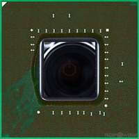
The GeForce GT 740M was a mobile graphics chip by NVIDIA, launched on April 1st, 2013. Built on the 28 nm process, and based on the GK107 graphics processor, in its GT 740M variant, the chip supports DirectX 12. Even though it supports DirectX 12, the feature level is only 11_0, which can be problematic with newer DirectX 12 titles. The GK107 graphics processor is an average sized chip with a die area of 118 mm² and 1,270 million transistors. It features 384 shading units, 32 texture mapping units, and 16 ROPs. NVIDIA has paired 2,048 MB DDR3 memory with the GeForce GT 740M, which are connected using a 128-bit memory interface. The GPU is operating at a frequency of 810 MHz, which can be boosted up to 895 MHz, memory is running at 901 MHz.
Being a mxm module card, the NVIDIA GeForce GT 740M does not require any additional power connector, its power draw is rated at 45 W maximum. This device has no display connectivity, as it is not designed to have monitors connected to it. Rather it is intended for use in laptop/notebooks and will use the output of the host mobile device. GeForce GT 740M is connected to the rest of the system using a PCI-Express 3.0 x16 interface.
Being a mxm module card, the NVIDIA GeForce GT 740M does not require any additional power connector, its power draw is rated at 45 W maximum. This device has no display connectivity, as it is not designed to have monitors connected to it. Rather it is intended for use in laptop/notebooks and will use the output of the host mobile device. GeForce GT 740M is connected to the rest of the system using a PCI-Express 3.0 x16 interface.
Graphics Processor
Mobile Graphics
- Release Date
- Apr 1st, 2013
- Generation
- GeForce 700M
- Predecessor
- GeForce 600M
- Successor
- GeForce 800M
- Production
- End-of-life
- Bus Interface
- PCIe 3.0 x16
Relative Performance
Based on TPU review data: "Performance Summary" at 1920x1080, 4K for 2080 Ti and faster.
Performance estimated based on architecture, shader count and clocks.
Clock Speeds
- Base Clock
- 810 MHz
- Boost Clock
- 895 MHz
- Memory Clock
-
901 MHz
1802 Mbps effective
Memory
- Memory Size
- 2 GB
- Memory Type
- DDR3
- Memory Bus
- 128 bit
- Bandwidth
- 28.83 GB/s
Render Config
- Shading Units
- 384
- TMUs
- 32
- ROPs
- 16
- SMX Count
- 2
- L1 Cache
- 16 KB (per SMX)
- L2 Cache
- 256 KB
Theoretical Performance
- Pixel Rate
- 7.160 GPixel/s
- Texture Rate
- 28.64 GTexel/s
- FP32 (float)
- 687.4 GFLOPS
- FP64 (double)
- 28.64 GFLOPS (1:24)
Board Design
- Slot Width
- MXM Module
- TDP
- 45 W
- Outputs
- Portable Device Dependent
- Power Connectors
- None
Graphics Features
- DirectX
- 12 (11_0)
- OpenGL
- 4.6
- OpenCL
- 3.0
- Vulkan
- 1.2.175
- CUDA
- 3.0
- Shader Model
- 6.5 (5.1)
GK107 GPU Notes
| NVENC: 1st Gen NVDEC: 1st Gen PureVideo HD: VP5 VDPAU: Feature Set D L1 Cache is configurable from 16 KB up to 48 KB per SMX Latest Drivers: Windows XP / Server 2003 x64: Quadro Release R319 U2 (321.01) Windows Vista: GeForce Release 365.19 Quadro Release R346 U7 (348.40) / R352 BETA (352.86) Windows 7 / 8 / 8.1 / 10 / 11 (x32 / x64): GeForce Release 391.35 / 475.06 Quadro Release R390 U9 (392.37) / R470 U16 (474.82) |
Dec 15th, 2024 19:41 EST
change timezone
Latest GPU Drivers
New Forum Posts
- What's your latest tech purchase? (22596)
- [Intel AX1xx/AX2xx/AX4xx/AX16xx/BE2xx/BE17xx] Intel Modded Wi-Fi Driver with Intel® Killer™ Features (218)
- nvidia gpu market share takes over 90% in Q4 2024 (Get's closer to full monopoly) (170)
- Post your mouse (42)
- How many are using 24h2? Problems still? (56)
- Lowering idle power on Zen 4? (48)
- Different low reading (54)
- TPU's F@H Team (20357)
- Are internal BD drives better than external ones? (15)
- Need help with PSU advice (7)
Popular Reviews
- Intel Arc B580 Review - Excellent Value
- ASRock Arc B580 Steel Legend Review
- Sparkle Arc B580 Titan OC Review
- AMD Ryzen 7 9800X3D Review - The Best Gaming Processor
- Intel Arc B580 Battlemage Unboxing & Preview
- ARCTIC P12 PWM PST A-RGB 120 mm Fan Review
- Upcoming Hardware Launches 2024 (Updated Nov 2024)
- be quiet! Light Base 600 LX Review
- STALKER 2 Performance Benchmark Review - 35 GPUs Tested
- AMD Ryzen 7 9700X Review - The Magic of Zen 5
Controversial News Posts
- Intel CEO Pat Gelsinger Retires, Company Appoints two Interim co-CEOs (217)
- AMD Radeon RX 8800 XT RDNA 4 Enters Mass-production This Month: Rumor (213)
- AMD Radeon RX 8800 XT Reportedly Features 220 W TDP, RDNA 4 Efficiency (122)
- NVIDIA GeForce RTX 5070 Ti Leak Tips More VRAM, Cores, and Power Draw (108)
- Microsoft is Introducing a $349 Mini PC That Streams Windows 11 from the Cloud (106)
- Intel 18A Process Node Clocks an Abysmal 10% Yield: Report (90)
- NVIDIA GeForce RTX 5070 Ti Specs Leak: Same Die as RTX 5080, 300 W TDP (88)
- Microsoft Loosens Windows 11 Install Requirements, TPM 2.0 Not Needed Anymore (83)

