Report an Error
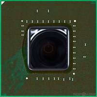
NVIDIA GeForce 820M
- Graphics Processor
- GK107
- Cores
- 384
- TMUs
- 32
- ROPs
- 16
- Memory Size
- 2 GB
- Memory Type
- DDR3
- Bus Width
- 128 bit
Recommended Gaming Resolutions:
- 1366x768
- 1600x900
- 1920x1080
The GeForce 820M is a mobile graphics chip by NVIDIA, launched on March 21st, 2015. Built on the 28 nm process, and based on the GK107 graphics processor, the chip supports DirectX 12. Even though it supports DirectX 12, the feature level is only 11_0, which can be problematic with newer DirectX 12 titles. The GK107 graphics processor is an average sized chip with a die area of 118 mm² and 1,270 million transistors. It features 384 shading units, 32 texture mapping units, and 16 ROPs. NVIDIA has paired 2,048 MB DDR3 memory with the GeForce 820M, which are connected using a 128-bit memory interface. The GPU is operating at a frequency of 810 MHz, memory is running at 901 MHz.
Being a mxm module card, its power draw is rated at 45 W maximum. This device has no display connectivity, as it is not designed to have monitors connected to it. Rather it is intended for use in laptop/notebooks and will use the output of the host mobile device. GeForce 820M is connected to the rest of the system using a PCI-Express 3.0 x16 interface.
Being a mxm module card, its power draw is rated at 45 W maximum. This device has no display connectivity, as it is not designed to have monitors connected to it. Rather it is intended for use in laptop/notebooks and will use the output of the host mobile device. GeForce 820M is connected to the rest of the system using a PCI-Express 3.0 x16 interface.
Graphics Processor
Mobile Graphics
- Release Date
- Mar 21st, 2015
- Generation
- GeForce 800M
- Predecessor
- GeForce 700M
- Successor
- GeForce 900M
- Production
- Active
- Bus Interface
- PCIe 3.0 x16
Relative Performance
Based on TPU review data: "Performance Summary" at 1920x1080, 4K for 2080 Ti and faster.
Performance estimated based on architecture, shader count and clocks.
Clock Speeds
- GPU Clock
- 810 MHz
- Memory Clock
-
901 MHz
1802 Mbps effective
Memory
- Memory Size
- 2 GB
- Memory Type
- DDR3
- Memory Bus
- 128 bit
- Bandwidth
- 28.83 GB/s
Render Config
- Shading Units
- 384
- TMUs
- 32
- ROPs
- 16
- SMX Count
- 2
- L1 Cache
- 16 KB (per SMX)
- L2 Cache
- 256 KB
Theoretical Performance
- Pixel Rate
- 6.480 GPixel/s
- Texture Rate
- 25.92 GTexel/s
- FP32 (float)
- 622.1 GFLOPS
- FP64 (double)
- 25.92 GFLOPS (1:24)
Board Design
- Slot Width
- MXM Module
- TDP
- 45 W
- Outputs
- Portable Device Dependent
Graphics Features
- DirectX
- 12 (11_0)
- OpenGL
- 4.6
- OpenCL
- 3.0
- Vulkan
- 1.2.175
- CUDA
- 3.0
- Shader Model
- 6.5 (5.1)
GK107 GPU Notes
| NVENC: 1st Gen NVDEC: 1st Gen PureVideo HD: VP5 VDPAU: Feature Set D L1 Cache is configurable from 16 KB up to 48 KB per SMX Latest Drivers: Windows XP / Server 2003 x64: Quadro Release R319 U2 (321.01) Windows Vista: GeForce Release 365.19 Quadro Release R346 U7 (348.40) / R352 BETA (352.86) Windows 7 / 8 / 8.1 / 10 / 11 (x32 / x64): GeForce Release 391.35 / 475.06 Quadro Release R390 U9 (392.37) / R470 U16 (474.82) |
Apr 7th, 2025 23:12 EDT
change timezone
Latest GPU Drivers
New Forum Posts
- Anyone with true HDDs still around here? (337)
- is it worth using ssd with usb2? (12)
- 28TB hard disk (30)
- Question about Intel Optane SSDs (70)
- USB case with dual USB-C and dual USB-A (6)
- The TPU UK Clubhouse (26058)
- Help me pick a UPS (88)
- 12v lines 0 reads occansionally (2)
- Someone run games on AMD BC-250 under Linux * Cut down PS5 die to 6 CPU cores 24 GPU cores for use in crypto mining (79)
- RX 9000 series GPU Owners Club (236)
Popular Reviews
- The Last Of Us Part 2 Performance Benchmark Review - 30 GPUs Compared
- UPERFECT UStation Delta Max Review - Two Screens In One
- ASUS Prime X870-P Wi-Fi Review
- PowerColor Radeon RX 9070 Hellhound Review
- Upcoming Hardware Launches 2025 (Updated Apr 2025)
- Sapphire Radeon RX 9070 XT Pulse Review
- MCHOSE L7 Pro Review
- Corsair RM750x Shift 750 W Review
- Sapphire Radeon RX 9070 XT Nitro+ Review - Beating NVIDIA
- DDR5 CUDIMM Explained & Benched - The New Memory Standard
Controversial News Posts
- NVIDIA GeForce RTX 5060 Ti 16 GB SKU Likely Launching at $499, According to Supply Chain Leak (161)
- MSI Doesn't Plan Radeon RX 9000 Series GPUs, Skips AMD RDNA 4 Generation Entirely (146)
- Microsoft Introduces Copilot for Gaming (124)
- AMD Radeon RX 9070 XT Reportedly Outperforms RTX 5080 Through Undervolting (119)
- NVIDIA Reportedly Prepares GeForce RTX 5060 and RTX 5060 Ti Unveil Tomorrow (115)
- Over 200,000 Sold Radeon RX 9070 and RX 9070 XT GPUs? AMD Says No Number was Given (100)
- NVIDIA GeForce RTX 5050, RTX 5060, and RTX 5060 Ti Specifications Leak (97)
- Nintendo Switch 2 Launches June 5 at $449.99 with New Hardware and Games (92)

