Report an Error
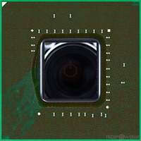
NVIDIA GeForce GT 640M
- Graphics Processor
- GK107
- Cores
- 384
- TMUs
- 32
- ROPs
- 16
- Memory Size
- 2 GB
- Memory Type
- DDR3
- Bus Width
- 128 bit
Recommended Gaming Resolutions:
- 1366x768
- 1600x900
- 1920x1080
The GeForce GT 640M was a mobile graphics chip by NVIDIA, launched on March 22nd, 2012. Built on the 28 nm process, and based on the GK107 graphics processor, in its N13P-GS variant, the chip supports DirectX 12. Even though it supports DirectX 12, the feature level is only 11_0, which can be problematic with newer DirectX 12 titles. The GK107 graphics processor is an average sized chip with a die area of 118 mm² and 1,270 million transistors. It features 384 shading units, 32 texture mapping units, and 16 ROPs. NVIDIA has paired 2,048 MB DDR3 memory with the GeForce GT 640M, which are connected using a 128-bit memory interface. The GPU is operating at a frequency of 624 MHz, which can be boosted up to 709 MHz, memory is running at 900 MHz.
Its power draw is rated at 32 W maximum. This device has no display connectivity, as it is not designed to have monitors connected to it. Rather it is intended for use in laptop/notebooks and will use the output of the host mobile device. GeForce GT 640M is connected to the rest of the system using a PCI-Express 3.0 x16 interface.
Its power draw is rated at 32 W maximum. This device has no display connectivity, as it is not designed to have monitors connected to it. Rather it is intended for use in laptop/notebooks and will use the output of the host mobile device. GeForce GT 640M is connected to the rest of the system using a PCI-Express 3.0 x16 interface.
Graphics Processor
Mobile Graphics
- Release Date
- Mar 22nd, 2012
- Generation
- GeForce 600M
- Predecessor
- GeForce 500M
- Successor
- GeForce 700M
- Production
- End-of-life
- Bus Interface
- PCIe 3.0 x16
- Reviews
- 2 in our database
Relative Performance
Based on TPU review data: "Performance Summary" at 1920x1080, 4K for 2080 Ti and faster.
Performance estimated based on architecture, shader count and clocks.
Clock Speeds
- Base Clock
- 624 MHz
- Boost Clock
- 709 MHz
- Memory Clock
-
900 MHz
1800 Mbps effective
Memory
- Memory Size
- 2 GB
- Memory Type
- DDR3
- Memory Bus
- 128 bit
- Bandwidth
- 28.80 GB/s
Render Config
- Shading Units
- 384
- TMUs
- 32
- ROPs
- 16
- SMX Count
- 2
- L1 Cache
- 16 KB (per SMX)
- L2 Cache
- 256 KB
Theoretical Performance
- Pixel Rate
- 5.672 GPixel/s
- Texture Rate
- 22.69 GTexel/s
- FP32 (float)
- 544.5 GFLOPS
- FP64 (double)
- 22.69 GFLOPS (1:24)
Board Design
- Slot Width
- IGP
- TDP
- 32 W
- Outputs
- Portable Device Dependent
- Power Connectors
- None
Graphics Features
- DirectX
- 12 (11_0)
- OpenGL
- 4.6
- OpenCL
- 3.0
- Vulkan
- 1.2.175
- CUDA
- 3.0
- Shader Model
- 6.5 (5.1)
Card Notes
| ???MHz core and 1000MHz memory clocks for the GDDR5 version, 625MHz/900MHz for the DDR3 version. |
GK107 GPU Notes
| NVENC: 1st Gen NVDEC: 1st Gen PureVideo HD: VP5 VDPAU: Feature Set D L1 Cache is configurable from 16 KB up to 48 KB per SMX Latest Drivers: Windows XP / Server 2003 x64: Quadro Release R319 U2 (321.01) Windows Vista: GeForce Release 365.19 Quadro Release R346 U7 (348.40) / R352 BETA (352.86) Windows 7 / 8 / 8.1 / 10 / 11 (x32 / x64): GeForce Release 391.35 / 475.06 Quadro Release R390 U9 (392.37) / R470 U16 (474.82) |
Jan 24th, 2025 00:16 EST
change timezone
Latest GPU Drivers
New Forum Posts
- NVIDIA RTX owners only - your opinion on DLSS 2.0 Image quality (393)
- HELP PLEASE - AMD 6700 XT BOOTING PROBLEM (34)
- 5090 AIB Clocks (0)
- 12700K vs 245K (44)
- RTX 5090 ridiculous price! (108)
- RDNA4 Prediction Time!!! (147)
- Audio starts crackling, then PC becomes unresponsive (16)
- What's your latest tech purchase? (22952)
- Free Games Thread (4401)
- Someone run games on AMD BC-250 under Linux * Cut down PS5 die to 6 CPU cores 24 GPU cores for use in crypto mining (57)
Popular Reviews
- NVIDIA GeForce RTX 5090 Founders Edition Review - The New Flagship
- NVIDIA GeForce RTX 5090 Founders Edition Unboxing
- NVIDIA GeForce RTX 5090 PCI-Express Scaling
- Alphacool Apex 1 CPU Water Block Review - Performance King!
- NZXT C1500 Review
- Pwnage StormBreaker Max CF Review
- PowerColor Alphyn AH10 Review
- AMD Ryzen 7 9800X3D Review - The Best Gaming Processor
- Montech Heritage Pro Review - The Leather Case
- NVIDIA GeForce RTX 50 Technical Deep Dive
Controversial News Posts
- NVIDIA 2025 International CES Keynote: Liveblog (470)
- AMD Debuts Radeon RX 9070 XT and RX 9070 Powered by RDNA 4, and FSR 4 (349)
- AMD Radeon RX 9070 XT & RX 9070 Custom Models In Stock at European Stores (226)
- NVIDIA GeForce RTX 5090 Features 575 W TDP, RTX 5080 Carries 360 W TDP (217)
- AMD Radeon RX 9070 XT Alleged Benchmark Leaks, Underwhelming Performance (204)
- AMD is Taking Time with Radeon RX 9000 to Optimize Software and FSR 4 (193)
- AMD's Radeon RX 9070 Launch Faces Pricing Hurdles (175)
- Potential RTX 5090 and RTX 5080 Pricing in China Leaks (173)

