Report an Error


NVIDIA GeForce GTX 670
- Graphics Processor
- GK104
- Cores
- 1344
- TMUs
- 112
- ROPs
- 32
- Memory Size
- 2 GB
- Memory Type
- GDDR5
- Bus Width
- 256 bit

GPU
I/O

Top

Bottom

Back

PCB Front

PCB Back
Recommended Gaming Resolutions:
- 1600x900
- 1920x1080
- 2560x1440
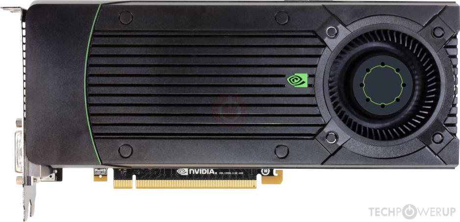
The GeForce GTX 670 was a high-end graphics card by NVIDIA, launched on May 10th, 2012. Built on the 28 nm process, and based on the GK104 graphics processor, in its GK104-325-A2 variant, the card supports DirectX 12. Even though it supports DirectX 12, the feature level is only 11_0, which can be problematic with newer DirectX 12 titles. The GK104 graphics processor is an average sized chip with a die area of 294 mm² and 3,540 million transistors. Unlike the fully unlocked GeForce GTX 680, which uses the same GPU but has all 1536 shaders enabled, NVIDIA has disabled some shading units on the GeForce GTX 670 to reach the product's target shader count. It features 1344 shading units, 112 texture mapping units, and 32 ROPs. NVIDIA has paired 2,048 MB GDDR5 memory with the GeForce GTX 670, which are connected using a 256-bit memory interface. The GPU is operating at a frequency of 915 MHz, which can be boosted up to 980 MHz, memory is running at 1502 MHz (6 Gbps effective).
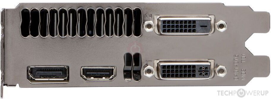
Being a dual-slot card, the NVIDIA GeForce GTX 670 draws power from 2x 6-pin power connectors, with power draw rated at 170 W maximum. Display outputs include: 2x DVI, 1x HDMI 1.4a, 1x DisplayPort 1.2. GeForce GTX 670 is connected to the rest of the system using a PCI-Express 3.0 x16 interface. The card's dimensions are 241 mm x 111 mm x 38 mm, and it features a dual-slot cooling solution. Its price at launch was 399 US Dollars.
Being a dual-slot card, the NVIDIA GeForce GTX 670 draws power from 2x 6-pin power connectors, with power draw rated at 170 W maximum. Display outputs include: 2x DVI, 1x HDMI 1.4a, 1x DisplayPort 1.2. GeForce GTX 670 is connected to the rest of the system using a PCI-Express 3.0 x16 interface. The card's dimensions are 241 mm x 111 mm x 38 mm, and it features a dual-slot cooling solution. Its price at launch was 399 US Dollars.
Graphics Processor
Graphics Card
- Release Date
- May 10th, 2012
- Generation
- GeForce 600
- Predecessor
- GeForce 500
- Successor
- GeForce 700
- Production
- End-of-life
- Launch Price
- 399 USD
- Bus Interface
- PCIe 3.0 x16
- Reviews
- 108 in our database
Relative Performance
Based on TPU review data: "Performance Summary" at 1920x1080, 4K for 2080 Ti and faster.
Clock Speeds
- Base Clock
- 915 MHz
- Boost Clock
- 980 MHz
- Memory Clock
-
1502 MHz
6 Gbps effective
Memory
- Memory Size
- 2 GB
- Memory Type
- GDDR5
- Memory Bus
- 256 bit
- Bandwidth
- 192.3 GB/s
Render Config
- Shading Units
- 1344
- TMUs
- 112
- ROPs
- 32
- SMX Count
- 7
- L1 Cache
- 16 KB (per SMX)
- L2 Cache
- 512 KB
Theoretical Performance
- Pixel Rate
- 27.44 GPixel/s
- Texture Rate
- 109.8 GTexel/s
- FP32 (float)
- 2.634 TFLOPS
- FP64 (double)
- 109.8 GFLOPS (1:24)
Board Design
- Slot Width
- Dual-slot
- Length
- 241 mm
9.5 inches
- Width
- 111 mm
4.4 inches
- Height
- 38 mm
1.5 inches
- TDP
- 170 W
- Suggested PSU
- 450 W
- Outputs
- 2x DVI
1x HDMI 1.4a
1x DisplayPort 1.2
- Power Connectors
- 2x 6-pin
- Board Number
- P2004 SKU 5
Graphics Features
- DirectX
- 12 (11_0)
- OpenGL
- 4.6
- OpenCL
- 3.0
- Vulkan
- 1.2.175
- CUDA
- 3.0
- Shader Model
- 6.5 (5.1)
GK104 GPU Notes
| NVENC: 1st Gen NVDEC: 1st Gen PureVideo HD: VP5 VDPAU: Feature Set D L1 Cache is configurable from 16 KB up to 48 KB per SMX Latest Drivers: Windows XP / Server 2003 x64: Quadro Release R319 U2 (321.01) Windows Vista: GeForce Release 365.19 Quadro Release R346 U7 (348.40) / R352 BETA (352.86) Windows 7 / 8 / 8.1 / 10 / 11 (x32 / x64): GeForce Release 391.35 / 475.06 Quadro Release R390 U9 (392.37) / R470 U16 (474.82) Data Center Release 427.11 Tesla Release 441.22 Windows 10 / 11 x64: GeForce Release 475.06 Quadro Release R470 U16 (474.82) Data Center Release 474.82 |
Retail boards based on this design (45)
| Name | GPU Clock | Boost Clock | Memory Clock | Other Changes |
|---|---|---|---|---|
| 915 MHz | 980 MHz | 1502 MHz | 272 mm/10.7 inches | |
| 915 MHz | 980 MHz | 1502 MHz | 4 GB, 272 mm/10.7 inches | |
| 980 MHz | 1058 MHz | 1502 MHz | 272 mm/10.7 inches | |
| 1059 MHz | 1137 MHz | 1502 MHz | 272 mm/10.7 inches | |
| 928 MHz | 1006 MHz | 1502 MHz | 170 mm/6.7 inches | |
| 1006 MHz | 1058 MHz | 1502 MHz | 256 mm/10.1 inches | |
| 915 MHz | 980 MHz | 1502 MHz | ||
| 915 MHz | 980 MHz | 1502 MHz | 207 mm/8.1 inches | |
| 967 MHz | 1046 MHz | 1502 MHz | 268 mm/10.6 inches | |
| 915 MHz | 980 MHz | 1502 MHz | 256 mm/10.1 inches | |
| 1006 MHz | 1084 MHz | 1552 MHz | 256 mm/10.1 inches | |
| 941 MHz | 1020 MHz | 1502 MHz | 256 mm/10.1 inches | |
| 1006 MHz | 1084 MHz | 1552 MHz | 256 mm/10.1 inches | |
| 1006 MHz | 1084 MHz | 1502 MHz | 4 GB, 256 mm/10.1 inches | |
| 967 MHz | 1046 MHz | 1502 MHz | 4 GB, 256 mm/10.1 inches | |
| 915 MHz | 980 MHz | 1502 MHz | 4 GB, 256 mm/10.1 inches | |
| 915 MHz | 980 MHz | 1502 MHz | 4 GB, 256 mm/10.1 inches | |
| 915 MHz | 980 MHz | 1502 MHz | 247 mm/9.7 inches | |
| 1006 MHz | 1084 MHz | 1527 MHz | 247 mm/9.7 inches | |
| 915 MHz | 980 MHz | 1502 MHz | ||
| 1006 MHz | 1084 MHz | 1502 MHz | 254 mm/10 inches | |
| 1006 MHz | 1084 MHz | 1502 MHz | 4 GB, 254 mm/10 inches | |
| 1006 MHz | 1084 MHz | 1502 MHz | 256 mm/10.1 inches | |
| 941 MHz | 1020 MHz | 1502 MHz | 265 mm/10.4 inches | |
| 980 MHz | 1058 MHz | 1502 MHz | 4 GB, 295 mm/11.6 inches, Triple-slot | |
| 915 MHz | 980 MHz | 1502 MHz | ||
| 1032 MHz | 1110 MHz | 1570 MHz | 4 GB, 255 mm/10 inches | |
| 1038 MHz | 1090 MHz | 1553 MHz | 255 mm/10 inches, Triple-slot | |
| 1006 MHz | 1084 MHz | 1553 MHz | 295 mm/11.6 inches, Triple-slot | |
| 1020 MHz | 1098 MHz | 1553 MHz | 4 GB, 295 mm/11.6 inches, Triple-slot | |
| 1006 MHz | 1084 MHz | 1502 MHz | 270 mm/10.6 inches | |
| 1006 MHz | 1084 MHz | 1502 MHz | 4 GB, 270 mm/10.6 inches | |
| 915 MHz | 980 MHz | 1502 MHz | ||
| 967 MHz | 1046 MHz | 1502 MHz | ||
| 1020 MHz | 1098 MHz | 1502 MHz | 267 mm/10.5 inches | |
| 915 MHz | 980 MHz | 1502 MHz | ||
| 915 MHz | 980 MHz | 1502 MHz | 247 mm/9.7 inches | |
| 1006 MHz | 1084 MHz | 1527 MHz | 247 mm/9.7 inches | |
| 915 MHz | 980 MHz | 1502 MHz | ||
| 954 MHz | 1032 MHz | 1552 MHz | ||
| 915 MHz | 980 MHz | 1502 MHz | ||
| 928 MHz | 1006 MHz | 1502 MHz | 4 GB, 254 mm/10 inches | |
| 1098 MHz | 1176 MHz | 1652 MHz | 254 mm/10 inches | |
| 1110 MHz | 1202 MHz | 1652 MHz | 284 mm/11.2 inches | |
| 954 MHz | 1032 MHz | 1502 MHz | 256 mm/10.1 inches, 2x DVI |


Apr 18th, 2025 14:08 EDT
change timezone
Latest GPU Drivers
New Forum Posts
- RX 9000 series GPU Owners Club (391)
- Can Intel recover in DYI market anytime soon? (2)
- GPU Database (300)
- Drives fail to work with Rufus Windows TO GO (2)
- Spoofer Modified SMBIOS/BIOS – Need Help Restoring Original Motherboard Info (TUF GAMING B550-PLUS WiFi II) (1)
- Current Sales, Bundles, Giveaways (10322)
- NVidia 576.02 breaks GPU temperature and rpm sensor read out and use for some applications (0)
- SK hynix A-Die (Overclocking thread) only for RYZEN AM5 users (66)
- Place your bets, what node will rtx 6000/RDNA 5(UDNA 1?) use (5)
- Is RX 9070 VRAM temperature regular value or hotspot? (363)
Popular Reviews
- ASUS GeForce RTX 5060 Ti TUF OC 16 GB Review
- NVIDIA GeForce RTX 5060 Ti PCI-Express x8 Scaling
- Palit GeForce RTX 5060 Ti Infinity 3 16 GB Review
- G.SKILL Trident Z5 NEO RGB DDR5-6000 32 GB CL26 Review - AMD EXPO
- ASUS GeForce RTX 5060 Ti Prime OC 16 GB Review
- Zotac GeForce RTX 5060 Ti AMP 16 GB Review
- MSI GeForce RTX 5060 Ti Gaming OC 16 GB Review
- Teevolution Terra Pro Review
- MSI GeForce RTX 5060 Ti Gaming Trio OC 16 GB Review
- ASUS GeForce RTX 5080 TUF OC Review
Controversial News Posts
- NVIDIA GeForce RTX 5060 Ti 16 GB SKU Likely Launching at $499, According to Supply Chain Leak (182)
- NVIDIA Sends MSRP Numbers to Partners: GeForce RTX 5060 Ti 8 GB at $379, RTX 5060 Ti 16 GB at $429 (127)
- Nintendo Confirms That Switch 2 Joy-Cons Will Not Utilize Hall Effect Stick Technology (105)
- Over 200,000 Sold Radeon RX 9070 and RX 9070 XT GPUs? AMD Says No Number was Given (100)
- Nintendo Switch 2 Launches June 5 at $449.99 with New Hardware and Games (99)
- NVIDIA Launches GeForce RTX 5060 Series, Beginning with RTX 5060 Ti This Week (98)
- Sony Increases the PS5 Pricing in EMEA and ANZ by Around 25 Percent (85)
- NVIDIA PhysX and Flow Made Fully Open-Source (77)