Report an Error


NVIDIA GeForce 8600 GTS
- Graphics Processor
- G84
- Cores
- 32
- TMUs
- 16
- ROPs
- 8
- Memory Size
- 256 MB
- Memory Type
- GDDR3
- Bus Width
- 128 bit

GPU
Recommended Gaming Resolutions:
- 640x480
- 1280x720
- 1366x768
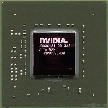
The GeForce 8600 GTS was a performance-segment graphics card by NVIDIA, launched on April 17th, 2007. Built on the 80 nm process, and based on the G84 graphics processor, in its G84-400-A2 variant, the card supports DirectX 11.1. Even though it supports DirectX 11, the feature level is only 10_0, which can be problematic with many DirectX 11 & DirectX 12 titles. The G84 graphics processor is an average sized chip with a die area of 169 mm² and 289 million transistors. It features 32 shading units, 16 texture mapping units, and 8 ROPs. NVIDIA has paired 256 MB GDDR3 memory with the GeForce 8600 GTS, which are connected using a 128-bit memory interface. The GPU is operating at a frequency of 675 MHz, memory is running at 1000 MHz.
Being a single-slot card, the NVIDIA GeForce 8600 GTS draws power from 1x 6-pin power connector, with power draw rated at 60 W maximum. Display outputs include: 2x DVI, 1x S-Video. GeForce 8600 GTS is connected to the rest of the system using a PCI-Express 1.0 x16 interface. The card measures 198 mm in length, and features a single-slot cooling solution. Its price at launch was 199 US Dollars.
Being a single-slot card, the NVIDIA GeForce 8600 GTS draws power from 1x 6-pin power connector, with power draw rated at 60 W maximum. Display outputs include: 2x DVI, 1x S-Video. GeForce 8600 GTS is connected to the rest of the system using a PCI-Express 1.0 x16 interface. The card measures 198 mm in length, and features a single-slot cooling solution. Its price at launch was 199 US Dollars.
Graphics Processor
Graphics Card
- Release Date
- Apr 17th, 2007
- Generation
-
GeForce 8
(8600)
- Predecessor
- GeForce 7 PCIe
- Successor
- GeForce 9
- Production
- End-of-life
- Launch Price
- 199 USD
- Bus Interface
- PCIe 1.0 x16
- Reviews
- 183 in our database
Relative Performance
Based on TPU review data: "Performance Summary" at 1920x1080, 4K for 2080 Ti and faster.
Performance estimated based on architecture, shader count and clocks.
Clock Speeds
- GPU Clock
- 675 MHz
- Shader Clock
- 1450 MHz
- Memory Clock
-
1000 MHz
2 Gbps effective
Memory
- Memory Size
- 256 MB
- Memory Type
- GDDR3
- Memory Bus
- 128 bit
- Bandwidth
- 32.00 GB/s
Render Config
- Shading Units
- 32
- TMUs
- 16
- ROPs
- 8
- SM Count
- 4
- L2 Cache
- 32 KB
Theoretical Performance
- Pixel Rate
- 5.400 GPixel/s
- Texture Rate
- 10.80 GTexel/s
- FP32 (float)
- 92.80 GFLOPS
Board Design
- Slot Width
- Single-slot
- Length
- 198 mm
7.8 inches
- TDP
- 60 W
- Suggested PSU
- 250 W
- Outputs
- 2x DVI
1x S-Video
- Power Connectors
- 1x 6-pin
- Board Number
- P401 SKU 0
Graphics Features
- DirectX
- 11.1 (10_0)
- OpenGL
- 3.3
- OpenCL
- 1.1
- Vulkan
- N/A
- CUDA
- 1.1
- Shader Model
- 4.0
Card Notes
| Memory Variant: 512 MB |
G84 GPU Notes
| PureVideo HD: VP2 VDPAU: Feature Set A Latest Drivers: Windows 2000: Quadro Release 261.19 Windows XP / Server 2003 x64: GeForce Release 185.81 (Notebooks) GeForce Release 340.52 Quadro Release R319 U2 (321.01) Tesla Release 258.96 Windows Vista: GeForce Release 307.83 (Notebooks) GeForce Release 342.01 Quadro Release R340 U15 (342.01) Tesla Release 258.96 Windows 7 / 8 / 8.1 / 10: GeForce Release 342.01 Quadro Release R340 U15 (342.01) Tesla Release 258.96 |
Retail boards based on this design (3)
| Name | GPU Clock | Memory Clock | Other Changes |
|---|---|---|---|
| 675 MHz | 1000 MHz | ||
| 720 MHz | 1100 MHz | 196 mm/7.7 inches | |
| 720 MHz | 1100 MHz |


Apr 10th, 2025 21:34 EDT
change timezone
Latest GPU Drivers
New Forum Posts
- Your PC ATM (35339)
- Post your cooling. (215)
- water chiller vs 480mm rad with water loop i9 13th gen cooling (3)
- I need help finding the correct vBIOS for my Chinese graphics card. It's an RX 580 (0)
- 7800x3D randomly hits 90C, readings make no sense? (10)
- TPU's F@H Team (20423)
- AMD RX580 2048SP on macOS - help! (2)
- New posts added to last post (automatic post merging) (28)
- Your GPU history? (372)
- TPU's Nostalgic Hardware Club (20221)
Popular Reviews
- The Last Of Us Part 2 Performance Benchmark Review - 30 GPUs Compared
- ASRock Z890 Taichi OCF Review
- Thermaltake TR100 Review
- Zotac GeForce RTX 5070 Ti Amp Extreme Review
- Sapphire Radeon RX 9070 XT Pulse Review
- Acer Predator GM9000 2 TB Review
- Sapphire Radeon RX 9070 XT Nitro+ Review - Beating NVIDIA
- Upcoming Hardware Launches 2025 (Updated Apr 2025)
- PowerColor Radeon RX 9070 Hellhound Review
- MCHOSE L7 Pro Review
Controversial News Posts
- NVIDIA GeForce RTX 5060 Ti 16 GB SKU Likely Launching at $499, According to Supply Chain Leak (175)
- MSI Doesn't Plan Radeon RX 9000 Series GPUs, Skips AMD RDNA 4 Generation Entirely (146)
- Microsoft Introduces Copilot for Gaming (124)
- AMD Radeon RX 9070 XT Reportedly Outperforms RTX 5080 Through Undervolting (119)
- NVIDIA Reportedly Prepares GeForce RTX 5060 and RTX 5060 Ti Unveil Tomorrow (115)
- NVIDIA Sends MSRP Numbers to Partners: GeForce RTX 5060 Ti 8 GB at $379, RTX 5060 Ti 16 GB at $429 (104)
- Nintendo Confirms That Switch 2 Joy-Cons Will Not Utilize Hall Effect Stick Technology (103)
- Over 200,000 Sold Radeon RX 9070 and RX 9070 XT GPUs? AMD Says No Number was Given (100)