Report an Error


NVIDIA GeForce 8500 GT
- Graphics Processor
- G86
- Cores
- 16
- TMUs
- 8
- ROPs
- 4
- Memory Size
- 256 MB
- Memory Type
- GDDR3
- Bus Width
- 128 bit

GPU
Recommended Gaming Resolutions:
- 640x480
- 1280x720
- 1366x768
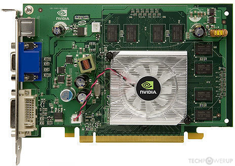
The GeForce 8500 GT was a mid-range graphics card by NVIDIA, launched on April 17th, 2007. Built on the 80 nm process, and based on the G86 graphics processor, in its G86-300-A2 variant, the card supports DirectX 11.1. Even though it supports DirectX 11, the feature level is only 10_0, which can be problematic with many DirectX 11 & DirectX 12 titles. The G86 graphics processor is an average sized chip with a die area of 127 mm² and 210 million transistors. It features 16 shading units, 8 texture mapping units, and 4 ROPs. NVIDIA has paired 256 MB GDDR3 memory with the GeForce 8500 GT, which are connected using a 128-bit memory interface. The GPU is operating at a frequency of 459 MHz, memory is running at 400 MHz.
Being a single-slot card, the NVIDIA GeForce 8500 GT does not require any additional power connector, its power draw is rated at 30 W maximum. Display outputs include: 1x DVI, 1x VGA, 1x S-Video. GeForce 8500 GT is connected to the rest of the system using a PCI-Express 1.0 x16 interface. The card measures 229 mm in length, and features a single-slot cooling solution. Its price at launch was 129 US Dollars.
Being a single-slot card, the NVIDIA GeForce 8500 GT does not require any additional power connector, its power draw is rated at 30 W maximum. Display outputs include: 1x DVI, 1x VGA, 1x S-Video. GeForce 8500 GT is connected to the rest of the system using a PCI-Express 1.0 x16 interface. The card measures 229 mm in length, and features a single-slot cooling solution. Its price at launch was 129 US Dollars.
Graphics Processor
Graphics Card
- Release Date
- Apr 17th, 2007
- Generation
-
GeForce 8
(8500)
- Predecessor
- GeForce 7 PCIe
- Successor
- GeForce 9
- Production
- End-of-life
- Launch Price
- 129 USD
- Bus Interface
- PCIe 1.0 x16
- Reviews
- 33 in our database
Relative Performance
Based on TPU review data: "Performance Summary" at 1920x1080, 4K for RTX 3080 and faster.
Performance estimated based on architecture, shader count and clocks.
Clock Speeds
- GPU Clock
- 459 MHz
- Shader Clock
- 918 MHz
- Memory Clock
-
400 MHz
800 Mbps effective
Memory
- Memory Size
- 256 MB
- Memory Type
- GDDR3
- Memory Bus
- 128 bit
- Bandwidth
- 12.80 GB/s
Render Config
- Shading Units
- 16
- TMUs
- 8
- ROPs
- 4
- SM Count
- 2
- L2 Cache
- 32 KB
Theoretical Performance
- Pixel Rate
- 1.836 GPixel/s
- Texture Rate
- 3.672 GTexel/s
- FP32 (float)
- 29.38 GFLOPS
Board Design
- Slot Width
- Single-slot
- Length
- 229 mm
9 inches
- TDP
- 30 W
- Suggested PSU
- 200 W
- Outputs
- 1x DVI
1x VGA
1x S-Video
- Power Connectors
- None
- Board Number
- P403
Graphics Features
- DirectX
- 11.1 (10_0)
- OpenGL
- 3.3
- OpenCL
- 1.1
- Vulkan
- N/A
- CUDA
- 1.1
- Shader Model
- 4.0
Card Notes
| Memory Variant: 512 MB Memory Variant: 1024 MB |
G86 GPU Notes
| PureVideo HD: VP2 VDPAU: Feature Set A Latest Drivers: Windows 2000: Quadro Release 261.19 Windows XP / Server 2003 x64: GeForce Release 185.81 (Notebooks) GeForce Release 340.52 Quadro Release R319 U2 (321.01) Tesla Release 258.96 Windows Vista: GeForce Release 307.83 (Notebooks) GeForce Release 342.01 Quadro Release R340 U15 (342.01) Tesla Release 258.96 Windows 7 / 8 / 8.1 / 10: GeForce Release 342.01 Quadro Release R340 U15 (342.01) Tesla Release 258.96 |
Retail boards based on this design (4)
| Name | GPU Clock | Memory Clock | Other Changes |
|---|---|---|---|
| 475 MHz | 475 MHz | DDR2 | |
| 600 MHz | 700 MHz | ||
| 600 MHz | 750 MHz | ||
| 700 MHz | 400 MHz | DDR2, 165 mm/6.5 inches |


Jul 18th, 2025 19:09 CDT
change timezone
Latest GPU Drivers
New Forum Posts
- What's your latest tech purchase? (24305)
- AI Job Losses: let's count the losses up, total losses to AI so far 94,000 and counting (35)
- lower score 5070Ti after replacing the PSU (0)
- TPU's Nostalgic Hardware Club (20539)
- 3DMARK "LEGENDARY" (329)
- Hatsune Miku x ASUS TUF Gaming Build (67)
- Anime Nation (13051)
- Ferrari themed mod cont. 4070s repaste (7)
- Stalker 2 is looking great. (213)
- Share your CPU-X Benchmarks! (6)
Popular Reviews
- Razer Blade 16 (2025) Review - Thin, Light, Punchy, and Efficient
- SilverStone SETA H2 Review
- Thermal Grizzly WireView Pro Review
- Pulsar X2 Crazylight Review
- MSI GeForce RTX 5060 Gaming OC Review
- Our Visit to the Hunter Super Computer
- NVIDIA GeForce RTX 5080 Founders Edition Review
- NVIDIA GeForce RTX 5050 8 GB Review
- Sapphire Radeon RX 9060 XT Pulse OC 16 GB Review - An Excellent Choice
- Upcoming Hardware Launches 2025 (Updated May 2025)
TPU on YouTube
Controversial News Posts
- Intel's Core Ultra 7 265K and 265KF CPUs Dip Below $250 (288)
- Some Intel Nova Lake CPUs Rumored to Challenge AMD's 3D V-Cache in Desktop Gaming (140)
- AMD Radeon RX 9070 XT Gains 9% Performance at 1440p with Latest Driver, Beats RTX 5070 Ti (131)
- NVIDIA Launches GeForce RTX 5050 for Desktops and Laptops, Starts at $249 (124)
- NVIDIA GeForce RTX 5080 SUPER Could Feature 24 GB Memory, Increased Power Limits (115)
- Microsoft Partners with AMD for Next-gen Xbox Hardware (105)
- NVIDIA DLSS Transformer Cuts VRAM Usage by 20% (99)
- AMD Sampling Next-Gen Ryzen Desktop "Medusa Ridge," Sees Incremental IPC Upgrade, New cIOD (97)