Report an Error


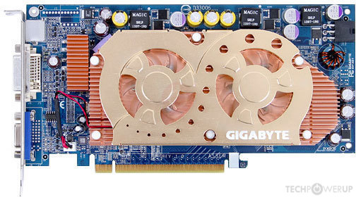
GIGABYTE 6600 GT 3D1
- GV-3D1
- Graphics Processor
- NV43 x2
- Pixel Shaders
- 8 x2
- Vertex Shaders
- 3 x2
- TMUs
- 8 x2
- ROPs
- 4 x2
- Memory Size
- 128 MB x2
- Memory Type
- GDDR3
- Bus Width
- 128 bit x2

GPU
Graphics Processor
Graphics Card
- Release Date
Aug 12th, 2004
Dec 28th, 2004
- Generation
-
GeForce 6 PCIe
(6600)
- Predecessor
- GeForce PCX
- Successor
- GeForce 7 PCIe
- Production
- End-of-life
- Bus Interface
- PCIe 1.0 x16
Clock Speeds
- GPU Clock
500 MHz
506 MHz (+1%)
- Memory Clock
-
560 MHz
566 MHz (+1%)
1120 Mbps effective
1132 Mbps effective
Memory
- Memory Size
- 128 MB
- Memory Type
- GDDR3
- Memory Bus
- 128 bit
- Bandwidth
-
17.92 GB/s
18.11 GB/s
Render Config
- Pixel Shaders
- 8
- Vertex Shaders
- 3
- TMUs
- 8
- ROPs
- 4
Theoretical Performance
- Pixel Rate
-
2.000 GPixel/s
2.024 GPixel/s
- Vertex Rate
-
375.0 MVertices/s
379.5 MVertices/s
- Texture Rate
-
4.000 GTexel/s
4.048 GTexel/s
Board Design
- Slot Width
- Single-slot
- TDP
- unknown
- Suggested PSU
- 200 W
- Outputs
- 1x DVI
1x VGA
1x S-Video
- Power Connectors
- 1x 6-pin
- Board Number
- P216
Graphics Features
- DirectX
- 9.0c (9_3)
- OpenGL
-
2.0 (full)
2.1 (partial)
- OpenCL
- N/A
- Vulkan
- N/A
- Shader Model
- 3.0
NV43 GPU Notes
| PureVideo HD: VP1 VDPAU: No Support Latest Drivers: Windows 2000: ForceWare Release 93.71 / 93.81 Beta Quadro Release 261.19 Windows XP / Server 2003 x64: GeForce Release 307.83 Quadro Release R310 U7 (312.69) Windows Vista / 7 / 8: GeForce Release 309.08 Quadro Release R310 U7 (312.69) |
Other retail boards based on this design (2)
| Name | GPU Clock | Memory Clock | Other Changes |
|---|---|---|---|
|
GIGABYTE 6600 GT 3D1

|
506 MHz | 566 MHz | |
| 500 MHz | 560 MHz |

Mar 11th, 2025 15:11 EDT
change timezone
Latest GPU Drivers
New Forum Posts
- GameTechBench GPU benchmark is already out! (314)
- Post your Old CDs, from back in the day thread. (43)
- 2006 Macbook Pro Modern Sleeper Project (0)
- Zen6 is almost here ? (49)
- Nvidia's GPU market share hits 90% in Q4 2024 (gets closer to full monopoly) (841)
- Avowed same FPS in every setting (1)
- TPU's Nostalgic Hardware Club (20079)
- Silent Hill Series Discussion/Speculation thread (1)
- As we live the age of game remakes, which game you would like to see to have a remake? (365)
- USB hard disk box capacity limits (16)
Popular Reviews
- Sapphire Radeon RX 9070 XT Nitro+ Review - Beating NVIDIA
- XFX Radeon RX 9070 XT Mercury OC Magnetic Air Review
- AMD Ryzen 9 9950X3D Review - Great for Gaming and Productivity
- ASUS Radeon RX 9070 TUF OC Review
- MSI MAG B850 Tomahawk Max Wi-Fi Review
- NVIDIA GeForce RTX 5070 Founders Edition Review
- Corsair Vengeance RGB CUDIMM DDR5-8800 48 GB CL42 Review
- AMD Ryzen 7 9800X3D Review - The Best Gaming Processor
- ASUS GeForce RTX 5070 Ti TUF OC Review
- MSI GeForce RTX 5070 Ti Gaming Trio OC+ Review
Controversial News Posts
- NVIDIA GeForce RTX 50 Cards Spotted with Missing ROPs, NVIDIA Confirms the Issue, Multiple Vendors Affected (513)
- AMD Radeon RX 9070 and 9070 XT Listed On Amazon - One Buyer Snags a Unit (261)
- AMD RDNA 4 and Radeon RX 9070 Series Unveiled: $549 & $599 (260)
- AMD Mentions Sub-$700 Pricing for Radeon RX 9070 GPU Series, Looks Like NV Minus $50 Again (248)
- NVIDIA Investigates GeForce RTX 50 Series "Blackwell" Black Screen and BSOD Issues (244)
- AMD Radeon RX 9070 and 9070 XT Official Performance Metrics Leaked, +42% 4K Performance Over Radeon RX 7900 GRE (195)
- AMD Radeon RX 9070-series Pricing Leaks Courtesy of MicroCenter (158)
- AMD Radeon RX 9070 XT Could Get a 32 GB GDDR6 Upgrade (100)