Report an Error
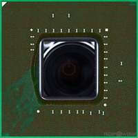
Dell GTX 660M
- Graphics Processor
- GK107
- Cores
- 384
- TMUs
- 32
- ROPs
- 16
- Memory Size
- 2 GB
- Memory Type
- GDDR5
- Bus Width
- 128 bit
Graphics Processor
Mobile Graphics
- Release Date
- Mar 22nd, 2012
- Generation
- GeForce 600M
- Predecessor
- GeForce 500M
- Successor
- GeForce 700M
- Production
- End-of-life
- Bus Interface
- MXM-B (3.0)
Clock Speeds
- Base Clock
- 835 MHz
- Boost Clock
- 950 MHz
- Memory Clock
-
1250 MHz
5 Gbps effective
Memory
- Memory Size
- 2 GB
- Memory Type
- GDDR5
- Memory Bus
- 128 bit
- Bandwidth
- 80.00 GB/s
Render Config
- Shading Units
- 384
- TMUs
- 32
- ROPs
- 16
- SMX Count
- 2
- L1 Cache
- 16 KB (per SMX)
- L2 Cache
- 256 KB
Theoretical Performance
- Pixel Rate
- 7.600 GPixel/s
- Texture Rate
- 30.40 GTexel/s
- FP32 (float)
- 729.6 GFLOPS
- FP64 (double)
- 30.40 GFLOPS (1:24)
Board Design
- Slot Width
- MXM Module
- TDP
- 50 W
- Outputs
- Portable Device Dependent
- Power Connectors
- None
- Board Number
- P1309 SKU 2
Graphics Features
- DirectX
- 12 (11_0)
- OpenGL
- 4.6
- OpenCL
- 3.0
- Vulkan
- 1.2.175
- CUDA
- 3.0
- Shader Model
- 6.5 (5.1)
GK107 GPU Notes
| NVENC: 1st Gen NVDEC: 1st Gen PureVideo HD: VP5 VDPAU: Feature Set D L1 Cache is configurable from 16 KB up to 48 KB per SMX Latest Drivers: Windows XP / Server 2003 x64: Quadro Release R319 U2 (321.01) Windows Vista: GeForce Release 365.19 Quadro Release R346 U7 (348.40) / R352 BETA (352.86) Windows 7 / 8 / 8.1 / 10 / 11 (x32 / x64): GeForce Release 391.35 / 475.06 Quadro Release R390 U9 (392.37) / R470 U16 (474.82) |
Other retail boards based on this design (2)
| Name | GPU Clock | Boost Clock | Memory Clock | Other Changes |
|---|---|---|---|---|
|
Dell GTX 660M

|
835 MHz | 950 MHz | 1250 MHz | |
| 835 MHz | 950 MHz | 1250 MHz |
Apr 1st, 2025 03:15 EDT
change timezone
Latest GPU Drivers
New Forum Posts
- DTS DCH Driver for Realtek HDA [DTS:X APO4 + DTS Interactive] (2122)
- 4070tisuper (10)
- AIO - 120mm cpu cooler? (38)
- Build complete! Any thoughts on undervolting? (20)
- Case fans work but can’t sync w/ rgb and stuck full rpm (1)
- Your PC ATM (35317)
- Undervolt i9-14900HX Laptop Newbie (8)
- Help with System Recommendations (5)
- can i yust connect 4 pin cpu coler to 5 pin ? (9)
- PCB serial number explanation Asrock rx5700xt Taichi oc+ (7)
Popular Reviews
- Sapphire Radeon RX 9070 XT Pulse Review
- DDR5 CUDIMM Explained & Benched - The New Memory Standard
- ASRock Phantom Gaming B850 Riptide Wi-Fi Review - Amazing Price/Performance
- Palit GeForce RTX 5070 GamingPro OC Review
- SilverStone Lucid 04 Review
- Samsung 9100 Pro 2 TB Review - The Best Gen 5 SSD
- Enermax REVOLUTION D.F. 12 850 W Review
- Sapphire Radeon RX 9070 XT Nitro+ Review - Beating NVIDIA
- Assassin's Creed Shadows Performance Benchmark Review - 30 GPUs Compared
- AMD Ryzen 7 9800X3D Review - The Best Gaming Processor
Controversial News Posts
- MSI Doesn't Plan Radeon RX 9000 Series GPUs, Skips AMD RDNA 4 Generation Entirely (142)
- Microsoft Introduces Copilot for Gaming (124)
- AMD Radeon RX 9070 XT Reportedly Outperforms RTX 5080 Through Undervolting (119)
- NVIDIA Reportedly Prepares GeForce RTX 5060 and RTX 5060 Ti Unveil Tomorrow (115)
- Over 200,000 Sold Radeon RX 9070 and RX 9070 XT GPUs? AMD Says No Number was Given (100)
- NVIDIA GeForce RTX 5050, RTX 5060, and RTX 5060 Ti Specifications Leak (96)
- Retailers Anticipate Increased Radeon RX 9070 Series Prices, After Initial Shipments of "MSRP" Models (90)
- China Develops Domestic EUV Tool, ASML Monopoly in Trouble (88)


