News Posts matching #2030

Return to Keyword Browsing

Intel 14A Node Delivers 15% Improvement over 18A, A14-E Adds Another 5%

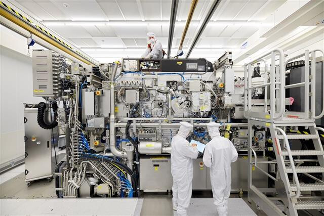
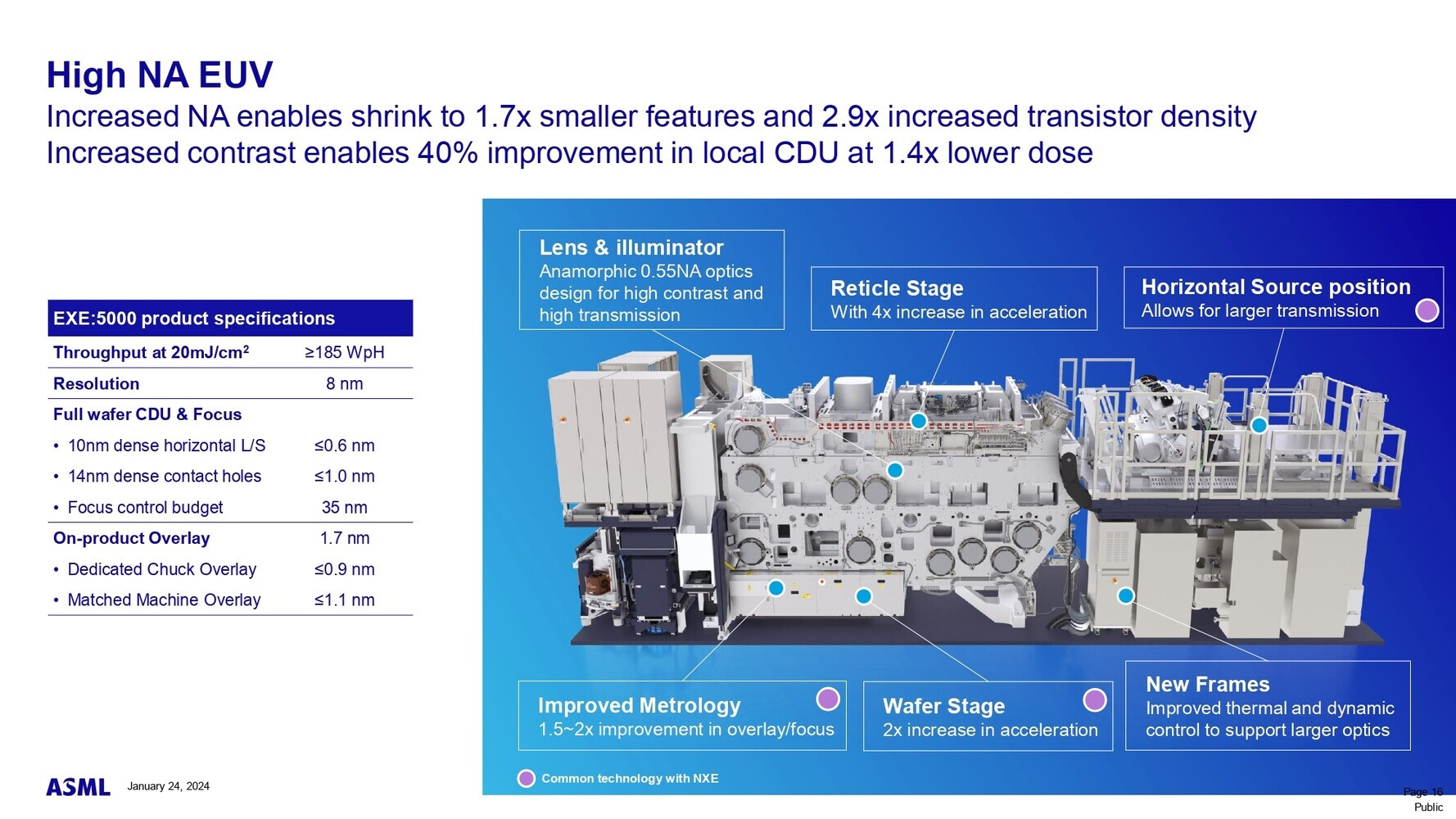
Intel is revamping its foundry play, and the company is set on its goals of becoming a strong contender to rivals such as TSMC and Samsung. Under Pat Gelsinger's lead, Intel recently split (virtually, under the same company) its units into Intel Product and Intel Foundry. During the SPIE 2024 conference for optics and photonics, Anne Kelleher, Intel's senior vice president, revealed that the 14A (1.4 nm) process offers a 15% performance-per-watt improvement over the company's 18A (1.8 nanometers) process. Additionally, the enhanced 14A-E process boasts a further 5% performance boost from the regular A14 node, being a small refresh. Intel's 14A process is set to be the first to utilize High-NA extreme ultraviolet (EUV) equipment, delivering a 20% increase in transistor logic density compared to the 18A node.

The company's aggressive pursuit of next-generation processes poses a significant threat to Samsung Electronics, which currently holds the second position in the foundry market. As part of its IDM 2.0 strategy, Intel hopes to reclaim its position as a leading foundry player and surpass Samsung by 2030. The company's collaboration with American companies, such as Microsoft, further solidifies its ambitions. Intel has already secured a $15 billion chip production contract with Microsoft for its 1.8 nm 18A process. The semiconductor industry is closely monitoring Intel's progress, as the company's advancements in process technology could potentially reshape the competitive landscape. With Samsung planning to mass-produce 2 nm process products next year, the race for dominance in the foundry market is heating up.

ASML High-NA EUV Twinscan EXE Machines Cost $380 Million, 10-20 Units Already Booked

ASML has revealed that its cutting-edge High-NA extreme ultraviolet (EUV) chipmaking tools, called High-NA Twinscan EXE, will cost around $380 million each—over twice as much as its existing Low-NA EUV lithography systems that cost about $183 million. The company has taken 10-20 initial orders from the likes of Intel and SK Hynix and plans to manufacture 20 High-NA systems annually by 2028 to meet demand. The High-NA EUV technology represents a major breakthrough, enabling an improved 8 nm imprint resolution compared to 13 nm with current Low-NA EUV tools. This allows chipmakers to produce transistors that are nearly 1.7 times smaller, translating to a threefold increase in transistor density on chips. Attaining this level of precision is critical for manufacturing sub-3 nm chips, an industry goal for 2025-2026. It also eliminates the need for complex double patterning techniques required presently.

However, superior performance comes at a cost - literally and figuratively. The hefty $380 million price tag for each High-NA system introduces financial challenges for chipmakers. Additionally, the larger High-NA tools require completely reconfiguring chip fabrication facilities. Their halved imaging field also necessitates rethinking chip designs. As a result, adoption timelines differ across companies - Intel intends to deploy High-NA EUV at an advanced 1.8 nm (18A) node, while TSMC is taking a more conservative approach, potentially implementing it only in 2030 and not rushing the use of these lithography machines, as the company's nodes are already developing well and on time. Interestingly, the installation process of ASML's High-NA Twinscan EXE 150,000-kilogram system required 250 crates, 250 engineers, and six months to complete. So, production is as equally complex as the installation and operation of this delicate machinery.

TSMC Allegedly Not Rushing into Adoption of High-NA EUV Machinery

DigiTimes Asia has reached out to insiders at fabrication toolmakers in an effort to delve deeper into claims made by industry analysts at the start of 2024—both SemiAnalysis and China Renaissance have proposed that TSMC is unlikely to adopt High-NA EUV production techniques within a five year period. The latest news article explores a non-upgrade approach for the next couple of years: "TSMC has not placed orders for high-numerical aperture (High-NA) extreme ultraviolet (EUV) tools and is unlikely to use the technology in 2 nm and 1.4 nm (A14) process manufacturing." Intel Foundry Services (IFS) will be one of the first semiconductor manufacturers to go online with ASML's latest and greatest machinery, although no firm timeframes have been confirmed. Team Blue's Taiwanese rival (and occasional business partner) is seemingly happy with its existing infrastructure, but industry watchdogs propose that cost considerations are key factors behind TSMC's cautious planning for the next decade.

The DigiTimes insider sources believe that TSMC will not budge until at least 2029, possibly coinciding with a 1 nm production node—analysts at China Renaissance reckon that High-NA EUV machines could be delivered in the future when facilities are readied for an "A10" codenamed process. TSMC published a very ambitious "transistor count" product timeline in early January (see below)—the first "1 nm" products are supposedly targeted for a 2030 rollout, but this schedule could change due to unforeseen circumstances. Intel is expected to "phase in" its fanciest ASML gear collection once the 18A process becomes old hat—Tom's Hardware thinks that 2026 - 2027 is a feasible timeframe.

AI Power Consumption Surge Strains US Electricity Grid, Coal-Powered Plants Make a Comeback

The artificial intelligence boom is driving a sharp rise in electricity use across the United States, catching utilities and regulators off guard. In northern Virginia's "data center alley," demand is so high that the local utility temporarily halted new data center connections in 2022. Nation-wide, electricity consumption at data centers alone could triple by 2030 to 390 TeraWatt Hours. Add in new electric vehicle battery factories, chip plants, and other clean tech manufacturing spurred by federal incentives, and demand over the next five years is forecast to rise at 1.5%—the fastest rate since the 1990s. Unable to keep pace, some utilities are scrambling to revise projections and reconsider previous plans of closing fossil fuel plants even as the Biden administration pushes for more renewable energy. Some older coal power plans will stay online, until the grid adds more power production capacity. The result could be increased emissions in the near term and risks of rolling blackouts if infrastructure continues lagging behind demand.

The situation is especially dire in Virginia, the world's largest data center hub. The state's largest utility, Dominion Energy, was forced to pause new data center connections for three months last year due to surging demand in Loudoun County. Though connections have resumed, Dominion expects load growth to almost double over the next 15 years. With data centers, EV factories, and other power-hungry tech continuing rapid expansion, experts warn the US national electricity grid is poorly equipped to handle the spike. Substantial investments in new transmission lines and generation are urgently needed to avoid businesses being turned away or blackouts in some regions. Though many tech companies aim to power operations with clean energy, factories are increasingly open to any available power source.

TSMC Plans to Put a Trillion Transistors on a Single Package by 2030

During the recent IEDM conference, TSMC previewed its process roadmap for delivering next-generation chip packages packing over one trillion transistors by 2030. This aligns with similar long-term visions from Intel. Such enormous transistor counts will come through advanced 3D packaging of multiple chipsets. But TSMC also aims to push monolithic chip complexity higher, ultimately enabling 200 billion transistor designs on a single die. This requires steady enhancement of TSMC's planned N2, N2P, N1.4, and N1 nodes, which are slated to arrive between now and the end of the decade. While multi-chipset architectures are currently gaining favor, TSMC asserts both packaging density and raw transistor density must scale up in tandem. Some perspective on the magnitude of TSMC's goals include NVIDIA's 80 billion transistor GH100 GPU—among today's largest chips, excluding wafer-scale designs from Cerebras.

Yet TSMC's roadmap calls for more than doubling that, first with over 100 billion transistor monolithic designs, then eventually 200 billion. Of course, yields become more challenging as die sizes grow, which is where advanced packaging of smaller chiplets becomes crucial. Multi-chip module offerings like AMD's MI300X and Intel's Ponte Vecchio already integrate dozens of tiles, with PVC having 47 tiles. TSMC envisions this expansion to chip packages housing more than a trillion transistors via its CoWoS, InFO, 3D stacking, and many other technologies. While the scaling cadence has recently slowed, TSMC remains confident in achieving both packaging and process breakthroughs to meet future density demands. The foundry's continuous investment ensures progress in unlocking next-generation semiconductor capabilities. But physics ultimately dictates timelines, no matter how aggressive the roadmap.

Fujitsu Details Monaka: 150-core Armv9 CPU for AI and Data Center

Ever since the creation of A64FX for the Fugaku supercomputer, Fujitsu has been plotting the development of next-generation CPU design for accelerating AI and general-purpose HPC workloads in the data center. Codenamed Monaka, the CPU is the latest creation for TSMC's 2 nm semiconductor manufacturing node. Based on Armv9-A ISA, the CPU will feature up to 150 cores with Scalable Vector Extensions 2 (SVE2), so it can process a wide variety of vector data sets in parallel. Using a 3D chiplet design, the 150 cores will be split into different dies and placed alongside SRAM and I/O controller. The current width of the SVE2 implementation is unknown.

The CPU is designed to support DDR5 memory and PCIe 6.0 connection for attaching storage and other accelerators. To bring cache coherency among application-specific accelerators, CXL 3.0 is present as well. Interestingly, Monaka is planned to arrive in FY2027, which starts in 2026 on January 1st. The CPU will supposedly use air cooling, meaning the design aims for power efficiency. Additionally, it is essential to note that Monaka is not a processor that will power the post-Fugaku supercomputer. The post-Fugaku supercomputer will use post-Monaka design, likely iterating on the design principles that Monaka uses and refining them for the launch of the post-Fugaku supercomputer scheduled for 2030. Below are the slides from Fujitsu's presentation, in Japenese, which highlight the design goals of the CPU.

US Government Announces $42 Billion Fund for Universal Access to High-Speed Broadband

The US government yesterday revealed its $42.45 billion Broadband Equity Access and Deployment (BEAD) funding program that will aim to deliver reliable, affordable high-speed internet to everyone in the nation by 2030—including all fifty states and US territories. Evidently parts of the country are lacking in terms of online access infrastructure—the briefing room statement outlines some of these issues: "High-speed internet is no longer a luxury - it is necessary for Americans to do their jobs, to participate equally in school, access health care, and to stay connected with family and friends. Yet, more than 8.5 million households and small businesses are in areas where there is no high-speed internet infrastructure, and millions more struggle with limited or unreliable internet options."

The initiative is said to be "the largest internet funding announcement in history," and the White House is readying packages valued from $27 million to $3.3 billion—White House said that it'll award sums of (starting at) $27 million going up to a maximum $3.3 billion, based on the required level of upgrades for a given state/territory. Assistant Secretary of Commerce for Communication and Information Alan Davidson stated: "This is a watershed moment for millions of people across America who lack access to a high-speed Internet connection. Access to Internet service is necessary for work, education, healthcare, and more...States can now plan their Internet access grant programs with confidence and engage with communities to ensure this money is spent where it is most needed."
Return to Keyword Browsing
May 1st, 2024 02:09 EDT change timezone

New Forum Posts

Popular Reviews

Controversial News Posts