News Posts matching #22 nm

Return to Keyword Browsing

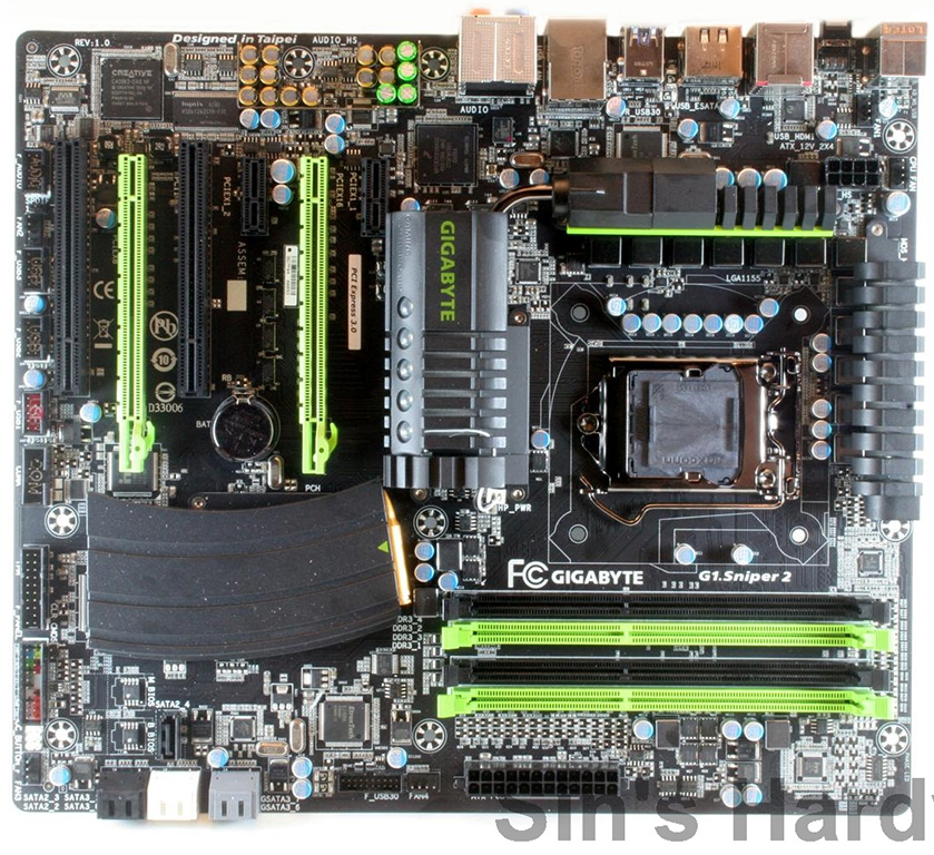
Production Gigabyte G1.Sniper 2 Features PCI-Express Gen. 3

About a month ago, we were treated to the first pictures of G1.Sniper 2, Gigabyte's first LGA1155 motherboard in its G1.Killer series of motherboards targeting the gamer-overclocker market segment. High resolution pictures showed the prototype of having PCI-Express Gen. 2 slots like most other LGA1155 boards. It turns out, according to a photo-session of a production sample by tech-blog SIN's Hardware, that Gigabyte refined the design with the production version (the one that will be sold in the markets), it features PCI-Express 3.0 (Gen. 3) graphics slots.

For a LGA1155 motherboard to have Gen. 3 PEG slots, it requires Gen. 3 specifications compliant switching circuitry, which wasn't available to motherboard vendors when they were designing their first LGA1155 boards. With availability of those components, motherboard vendors are not wasting any time in rolling out new variants of their LGA1155 boards that feature Gen. 3 PCI-Express slots. Gigabyte placed "PCI-Express 3.0" marking on the board manually using stickers, going on to show that adding Gen. 3 slots indeed may have been a last-minute decision at Gigabyte. The other interesting marking on the G1.Sniper 2 carton is the mention of the board being ready for upcoming 22 nm "Ivy Bridge" Core processors. More pictures, and a preview at the source.

MSI New Z68A-GD80 Swims in PCI-Express 3.0 Fame

While Sandy Bridge-E LGA2011 processors will come with integrated PCI-Express 3.0 hubs, they're still a couple of quarter financial years away. Meanwhile, MSI jumped the gun on its latest socket LGA1155 Intel Z68-based motherboard with not only support for Intel's upcoming 22 nm Ivy Bridge LGA1155 processors, but also the PCI-Express 3.0 hubs that the new processors come with. While Ivy Bridge has PCI-E 3.0 hub, not just any LGA1155 motherboard can give you PCI-E 3.0 support. It requires slots that are compliant with the new specification, and needs PCI-E 3.0 compliant external switching chips. MSI has both, on its new Z68A-GD80 motherboard, and with it, the bragging rights of being the world's first PCI-E 3.0 compliant motherboard.

PCI-Express 3.0 gives you twice the interface bandwidth as PCI-Express 2.0, which means that PCI-Express 3.0 x8 has the same bandwidth as PCI-Express 2.0 x16. But before you celebrate, let's remind ourselves that you also need a PCI-E 3.0 compliant GPU to make the slots operate at Gen 3.0 speeds. Installing PCI-Express 2.0 GPUs on Gen 3.0 won't run the slots at Gen 3.0 speeds. That aside, the Z68A-GD80 is a sufficiently-equipped enthusiast motherboard featuring 14-phase VRM for the CPU, dual-channel DDR3-2133 support, two PCI-E 3.0 x16 slots (x8/x8 with populated), a third PCI-E x16 wired to the Z68 PCH, running at PCI-E 2.0 x4 speeds, and a couple of PCI-E 2.0 x1 and legacy PCI. There are three internal SATA 6 Gb/s ports; eSATA, USB 3.0, make for the rest of the connectivity. There is full-fledged display connectivity, with Lucid Virtu support. Expect this board to be out any time soon.

Intel Accelerating Ivy Bridge Unveiling to Computex 2011

Intel is preparing to unveil its next-generation processors based on the Ivy Bridge architecture as early as by Computex 2011 (May 30 to June 4), according to Commercial Times, a Chinese language business newspaper. Ivy Bridge is an optical shrink of the Sandy Bridge architecture, processors based on it will be manufactured on the 22 nanometer silicon fabrication process. Intel launched its Sandy Bridge 32 nm processors at CES 2011, in January. In related news from the same source, AMD has also accelerated the production of its Llano APUs and is expected to begin shipping the APUs to ODM/OEM makers in May at the earliest instead of the original schedule set in the third quarter.

Intel Announces Multi-Billion-Dollar Investment in Next-Gen. Manufacturing in U.S.

Intel Corporation announced today that the company will invest between $6 billion and $8 billion on future generations of manufacturing technology in its American facilities. The action will fund deployment of Intel's next-generation 22- nanometer (nm) manufacturing process across several existing U.S. factories, along with construction of a new development fabrication plant (commonly called a "fab") in Oregon. The projects will support 6,000 to 8,000 construction jobs and result in 800 to 1,000 new permanent high-tech jobs.

"Today's announcement reflects the next tranche of the continued advancement of Moore's Law and a further commitment to invest in the future of Intel and America," said Intel President and CEO Paul Otellini. "The most immediate impact of our multi-billion-dollar investment will be the thousands of jobs associated with building a new fab and upgrading four others, and the high-wage, high-tech manufacturing jobs that follow."

GLOBALFOUNDRIES Breaks Ground on World's Most Advanced Semiconductor Foundry

GLOBALFOUNDRIES today announced it officially broke ground on the construction of Fab 2, a new semiconductor manufacturing facility located at the Luther Forest Technology Campus in Saratoga County, New York. Once completed, Fab 2 will stand as the most technologically advanced semiconductor manufacturing facility, or fab, in the world and the largest leading-edge semiconductor foundry in the United States. The construction and ramp-up phases for the new $4.2 billion facility are expected to take approximately three years to complete, with volume production expected in 2012.

"Semiconductors are the building blocks of technology innovation and are present in everything from mobile phones to kitchen appliances and solar panels," said Hector Ruiz, chairman of GLOBALFOUNDRIES. "As today's chip designers push the boundaries on the next generation of products, there is a growing need for a new approach to design and manufacturing rooted in collaboration and innovation. With Fab 2, GLOBALFOUNDRIES moves the semiconductor industry away from the traditional model of isolated regional development and into an era of global hubs of manufacturing and technology expertise."

GLOBALFOUNDRIES Calls for Renewed Focus on 300 mm Manufacturing Innovation

In its effort to meet the ever-increasing demands of consumer technology, the semiconductor industry has long been preoccupied with smaller transistors and larger silicon wafers. While these are important tactics, opportunities for increasing efficiency, becoming more agile, and minimizing waste are often overlooked in manufacturing processes, according to Thomas Sonderman, vice president of manufacturing systems and technology at GLOBALFOUNDRIES.

At SEMICON West 2009, Sonderman is calling for a renewed focus on operational agility in the semiconductor manufacturing industry, particularly in light of increased pressure to move to processes based on 450 millimeter (mm) wafers.

GLOBALFOUNDRIES Details Advanced Technology Aimed at 22 nm and Beyond

GLOBALFOUNDRIES today described an innovative technology that could overcome one of the key hurdles to advancing high-k metal gate (HKMG) transistors, bringing the industry one step closer to the next generation of mobile devices with more computing power and vastly improved battery life.

The semiconductor industry is celebrated for overcoming seemingly insurmountable odds to continue the trend toward smaller, faster, and more energy-efficient products. Performed in partnership with IBM through GLOBALFOUNDRIES' participation in the IBM Technology Alliance, the new research is designed to enable the continued scaling of semiconductor components to the 22 nanometer node and beyond.

IBM and AMD First to Reach the 22 nm Silicon Fabrication Mark

IBM and its chip development partners announced today that they've developed the first functional 22nm silicon fabricated SRAM cell. This puts them ahead of Intel, which had announced its technological entry into the 32 nm domain in September, 2007. SRAM is usually the first semiconductor device a chip-maker tests a new fabrication-process on, before working on microprocessors. These devices were developed and manufactured by AMD, Freescale, IBM STMicroelectronics, Toshiba and the College of Nanoscale Science and Engineering (CNSE). They were built in the conventional 6-transistor design and on a 300 mm wafer. This level of miniaturization made the SRAM cell shrink to a mere 0.1 sq. μm, compare this to the SRAM cells that go into making caches on the 45 nm Intel processors, 0.346 sq. μm.
Return to Keyword Browsing
May 21st, 2024 18:26 EDT change timezone

New Forum Posts

Popular Reviews

Controversial News Posts