News Posts matching #3D

Return to Keyword Browsing

BBCube 3D Could be the Future of Stacked DRAM

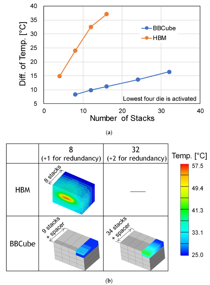
Scientists at the Tokyo Institute of Technology have developed a new type of stacked or 3D DRAM that the researchers call Bumpless Build Cube 3D or BBCube 3D, which relies on Through Silicon Vias or TSVs to connect the DRAM dies. This is a different approach to HBM which relies on micro bumps to connect the layers together and the Japanese scientists are saying that their bumpless wafer-on-wafer solution should allow not only for an easier manufacturing process, but more importantly, improved cooling, as the TSVs can channel the heat from the DRAM dies down into whatever substrate the BBCube 3D stack is finally mounted onto.

If that wasn't enough, the researchers believe that BBCube 3D will be able to deliver higher speeds than HBM courtesy of a combination of the TSVs being relatively short and "high-density signal parallelism". BBCube 3D is expected to deliver up to a 32 fold increase in bandwidth compared to DDR5 memory and a four fold increase compared to HBM2E memory, while at the same time, drawing less power. The research paper goes into a lot more details for those interested at taking a closer look at this potentially revolutionary shift in DRAM assembly. However, the question that remains unanswered is if this will end up as a real world product some time in the near future, which is all based on how manufacturable BBCube 3D memory will be.

Lam Research Introduces World's First Bevel Deposition Solution to Increase Yield in Chip Production

Lam Research Corp. (Nasdaq: LRCX) today introduced Coronus DX, the industry's first bevel deposition solution optimized to address key manufacturing challenges in next-generation logic, 3D NAND and advanced packaging applications. As semiconductors continue to scale, manufacturing becomes increasingly complex with hundreds of process steps needed to build nanometer-sized devices on a silicon wafer. In a single step, Coronus DX deposits a proprietary layer of protective film on both sides of the wafer edge that helps prevent defects and damage that can often occur during advanced semiconductor manufacturing. This powerful protection increases yield and enables chipmakers to implement new leading-edge processes for the production of next-generation chips. Coronus DX is the newest addition to the Coronus product family and extends Lam's leadership in bevel technology.

"In the era of 3D chipmaking, production is complex and costly," said Sesha Varadarajan, senior vice present of the Global Products Group at Lam Research. "Building on Lam's expertise in bevel innovation, Coronus DX helps drive more predictable manufacturing and significantly higher yield, paving the way for adoption of advanced logic, packaging and 3D NAND production processes that weren't previously feasible."

NVIDIA H100 Hopper GPU Tested for Gaming, Slower Than Integrated GPU

NVIDIA's H100 Hopper GPU is a device designed for pure AI and other compute workloads, with the least amount of consideration for gaming workloads that involve graphics processing. However, it is still interesting to see how this 30,000 USD GPU fairs in comparison to other gaming GPUs and whether it is even possible to run games on it. It turns out that it is technically feasible but not making much sense, as the Chinese YouTube channel Geekerwan notes. Based on the GH100 GPU SKU with 14,592 CUDA, the H100 PCIe version tested here can achieve 204.9 TeraFLOPS at FP16, 51.22 TeraFLOPS at FP32, and 25.61 TeraFLOPS at FP64, with its natural power laying in accelerating AI workloads.

However, how does it fare in gaming benchmarks? Not very well, as the testing shows. It scored 2681 points in 3DMark Time Spy, which is lower than AMD's integrated Radeon 680M, which managed to score 2710 points. Interestingly, the GH100 has only 24 ROPs (render output units), while the gaming-oriented GA102 (highest-end gaming GPU SKU) has 112 ROPs. This is self-explanatory and provides a clear picture as to why the H100 GPU is used for computing only. Since it doesn't have any display outputs, the system needed another regular GPU to provide the picture, while the computation happened on the H100 GPU.

AMD's Dr. Lisa Su Thinks That Moore's Law is Still Relevant - Innovation Will Keep Legacy Going

Barron's Magazine has been on a technology industry kick this week and published their interview with AMD CEO Dr. Lisa Su on May 3. The interviewer asks Su about her views on Moore's Law and it becomes apparent that she remains a believer of Gordon Moore's (more than half-century old) prediction - Moore, an Intel co-founder passed away in late March. Su explains that her company's engineers will need to innovate in order to carry on with that legacy: "I would certainly say I don't think Moore's Law is dead. I think Moore's Law has slowed down. We have to do different things to continue to get that performance and that energy efficiency. We've done chiplets - that's been one big step. We've now done 3-D packaging. We think there are a number of other innovations, as well." Expertise in other areas is also key in hitting technological goals: "Software and algorithms are also quite important. I think you need all of these pieces for us to continue this performance trajectory that we've all been on."

When asked about the challenges involved in advancing CPU designs within limitations, Su responds with: "Yes. The transistor costs and the amount of improvement you're getting from density and overall energy reduction is less from each generation. But we're still moving (forward) generation to generation. We're doing plenty of work in 3 nanometer today, and we're looking beyond that to 2 nm as well. But we'll continue to use chiplets and these type of constructions to try to get around some of the Moore's Law challenges." AMD and Intel continue to hold firm with Moore's Law, even though slightly younger upstarts disagree (see NVIDIA). Dr. Lisa Su's latest thoughts stay consistent with her colleague's past statements - AMD CTO Mark Papermaster reckoned that the theory is pertinent for another six to eight years, although it could be a costly endeavor for AMD - the company believes that it cannot double transistor density every 18 to 24 months without incurring extra expenses.

NEO Semiconductor Launches Ground-Breaking 3D X-DRAM Technology, A Game Changer in the Memory Industry

NEO Semiconductor, a leading developer of innovative technologies for 3D NAND flash and DRAM memory, today announced the launch of its ground-breaking technology, 3D X-DRAM. This development is the world's first 3D NAND-like DRAM cell array that is targeted to solve DRAM's capacity bottleneck and replace the entire 2D DRAM market. Relevant patent applications were published with the United States Patent Application Publication on April 6, 2023.

"3D X-DRAM will be the absolute future growth driver for the Semiconductor industry," said Andy Hsu, Founder and CEO of NEO Semiconductor and an accomplished technology inventor with more than 120 U.S. patents. "Today I can say with confidence that Neo is becoming a clear leader in the 3D DRAM market. Our invention, compared to the other solutions in the market today, is very simple and less expensive to manufacture and scale. The industry can expect to achieve 8X density and capacity improvements per decade with our 3D X-DRAM."

TSMC Certifies Ansys Multiphysics Solutions for TSMC's N2 Silicon Process

Ansys and TSMC continue their long-standing technology collaboration to announce the certification of Ansys' power integrity software for TSMC's N2 process technology. The TSMC N2 process, which adopts nanosheet transistor structure, represents a major advancement in semiconductor technology with significant speed and power advantages for high performance computing (HPC), mobile chips, and 3D-IC chiplets. Both Ansys RedHawk-SC and Ansys Totem are certified for power integrity signoff on N2, including the effects of self-heat on long-term reliability of wires and transistors. This latest collaboration builds on the recent certification of the Ansys platform for TSMC's N4 and N3E FinFLEX processes.

"TSMC works closely with our Open Innovation Platform (OIP) ecosystem partners to help our mutual customers achieve the best design results with the full stack of design solutions on TSMC's most advanced N2 process," said Dan Kochpatcharin, head of the Design Infrastructure Management Division at TSMC. "Our latest collaboration with Ansys RedHawk-SC and Totem analysis tools allows our customers to benefit from the significant power and performance improvements of our N2 technology while ensuring predictively accurate power and thermal signoff for the long-term reliability of their designs."

Synopsys, TSMC and Ansys Strengthen Ecosystem Collaboration to Advance Multi-Die Systems

Accelerating the integration of heterogeneous dies to enable the next level of system scalability and functionality, Synopsys, Inc. (Nasdaq: SNPS) has strengthened its collaboration with TSMC and Ansys for multi-die system design and manufacturing. Synopsys provides the industry's most comprehensive EDA and IP solutions for multi-die systems on TSMC's advanced 7 nm, 5 nm and 3 nm process technologies with support for TSMC 3DFabric technologies and 3Dblox standard. The integration of Synopsys implementation and signoff solutions and Ansys multi-physics analysis technology on TSMC processes allows designers to tackle the biggest challenges of multi-die systems, from early exploration to architecture design with signoff power, signal and thermal integrity analysis.

"Multi-die systems provide a way forward to achieve reduced power and area and higher performance, opening the door to a new era of innovation at the system-level," said Dan Kochpatcharin, head of Design Infrastructure Management Division at TSMC. "Our long-standing collaboration with Open Innovation Platform (OIP) ecosystem partners like Synopsys and Ansys gives mutual customers a faster path to multi-die system success through a full spectrum of best-in-class EDA and IP solutions optimized for our most advanced technologies."

Bizarre Open World FPS The Explorator Showcased in ID@Xbox Trailer

Explore the world of Ospolis and discover fabulous treasures in this comic book style FPS. The Explorator is a game inspired by oldschool FPS with a cell shading visual style, as an explorer you take your courage in both hands to set foot on the most dangerous island of the known world, Ospolis.

Legends say that the legendary city of Atlantis lies beneath this island, which has been suddenly overrun by goblins and monsters that have emerged from the bowels of the underground tunnels drilled by unwary explorers confident of finding this famous city. Explore mysterious counter-zones and brave dangers to discover priceless treasures buried beneath the ruins of Atlantis.

AMD EPYC Genoa-X Processor Spotted with 1248 MBs of 3D V-Cache

AMD's EPYC lineup already features the new Zen 4 core designed for better performance and efficiency. However, since the release of EPYC Milan-X processors with 3D V-cache integrated into server offerings, we wondered if AMD will continue to make such SKUs for upcoming generations. According to the report from Wccftech, we have a leaked table of specifications that showcase what some seemingly top-end Genoa-X SKUs will look like. The two SKUs listed here are the "100-000000892-04" coded engineering sample and the "100-000000892-06" coded retail sample. With support for the same SP5 platform, these CPUs should be easily integrated with the existing offerings from OEM.

As far as specifications, this processor features 384 MBs of L3 cache coming from CCDs, 768 MBs of L3 cache from the 3D V-Cache stacks, and 96 MBs of L2 cache for a total of 1248 MBs in the usable cache. A 3 MB stack of L1 cache is also dedicated to instructions and primary CPU data. Compared to the regular Genoa design, this is a 260% increase in cache sizes, and compared to Milan-X, the Genoa-X design also progresses with 56% more cache. With a TDP of up to 400 Watts, configurable to 320 Watts, this CPU can boost up to 3.7 GHz. AMD EPYC Genoa-X CPUs are expected to hit the shelves in the middle of 2023.

Acer to Share Game-Changing Stereo 3D Gaming Advancements with SpatialLabs at GDC 2023

Acer will be participating in the Game Developers Conference (GDC) 2023 held from March 20-24 in San Francisco to share the latest innovations of its industry-leading SpatialLabs experience. It combines advanced eye-tracking cameras, a stereoscopic 3D display and stereo rendering capabilities to deliver immersive 3D experiences without the need for specialized glasses. With a click of a button, 2D visuals seem to pop out of their screens, giving designers, marketers, and other professionals a unique way of interacting with their creations in 3D views.

SpatialLabs TrueGame
Following its launch in 2021, Acer took it up a notch by bringing its glasses-free stereoscopic 3D technology to the world of gaming through the SpatialLabs TrueGame application. With a Predator Helios 300 SpatialLabs Edition laptop, or a SpatialLabs View display paired with a PC, users can enjoy the supported titles in their true 3D form, delivering immersive gaming experiences as envisioned by their developers. This is possible because games are mostly created with a three-dimensional world in mind as developers include information about depth in each scene and object they build. SpatialLabs leverages this already-existing information in order to present the games in stereoscopic 3D. A dedicated pre-configured profile is now available for each game title, among the 70+ modern and classic titles on launch, to offer players a seamless experience with their favorite games. More profiles for additional titles will be added on a continuous basis moving forward.

300 TB SSDs Could Arrive as Soon as 2026, Claims Pure Storage

Pure Storage, a maker of various storage solutions and custom enterprise-grade SSDs, claims the company will produce SSDs with up to 300 TBs of capacity by 2026. In an interview with Pure Storage CTO Alex McMullan, Blocks & Files got exclusive information that the company targets SSD capacities of up to 300 TBs in 2026. Pure Storage creates proprietary Direct Flash Modules (DFM) SSDs which use 3D NAND chips controlled by a custom SSD controller, are used in the FlashArray systems, and run on a custom FlashBlade operating system. This level of customization allows Pure Storage to create SSD drives with remarkable capacities in the future as the 3D NAND technology advances.

In the coming years, 3D NAND flash manufacturers will switch from the current 200-layer chips to the 400/500-layer chips, driving storage density to new highs. As manufacturers update their technology, so does Pure with its DFM cards that use regular U.2 NVMe connectors in a custom ruler-style format made explicitly for Pure FlashArray systems. Compared to upcoming HDDs that Toshiba and Seagate will use, Pure Storage DFM SSDs will have much higher capacities and read/write speeds, especially as higher-density 3D NAND arrives. You can see the comparison of Pure's estimates for the future 300 TB SSDs with future HDD technology.

Reservations Open for World's First AI-Powered 3D Tablet: Award-Winning Lume Pad 2 by Leia Inc

The future of 3D viewing is here: United States reservations are now open for Leia Inc.'s Lume Pad 2, the world's first 3D•AI tablet equipped with embedded technology to create fully immersive 3D calling, streaming, and gaming experiences along with content sharing and creation apps - all without the need for any eyewear. Starting today, the Lume Pad 2 is available for reservation via LeiaInc.com at a suggested retail price of $1,099. Customers who reserve before March 31 will receive a $100 discount when they confirm their order in April, when tablets begin shipping.

"With Leia's unique 3D•AI experiences, now available worldwide, people no longer have to settle for unnatural interactions like video chat on a flat screen," said Cecilia Qvist, CEO, Leia Inc. "Lume Pad 2 is for anyone who has ever sought a more genuine human connection from their online experiences." "We know that 3D isn't new - but how we do it is," said David Fattal, Leia Inc. co-founder and CTO. "With the world focused on how AI will continue to shape our future, we feel that this is one of its most thrilling applications - giving the naked eye a fully immersive 3D viewing experience that we believe makes Lume Pad 2 a 3D device for everyone."

AMD Ryzen 9 7950X3D Runs First Benchmarks

AMD's upcoming Ryzen 9 7950X3D processor will bring 16 cores and 32 threads along with 16 MB of L2 cache and 128 MB of L3 cache for 144 MB of 3D V-cache present on the package. Today, we get to see it in action for the first time in benchmarks like Blender for 3D content creation and Geekbench 5 for synthetic benchmarks, where we get to compare the scores to the already existing models. In Blender, the new AMD Ryzen 9 7950X3D scores 558.59 points, while the regular Ryzen 9 7950X scores 590.28 points. This represents a 5.4% regression from the original model; however, we are yet to see how other content creation benchmarks suit the new CPU.

For Geekbench 5 synthetics, the upcoming Ryzen 9 7950X3D scores 2,157 points in the single-core score and 21,841 points in the multi-core score. The regular Ryzen 9 7950X can reach around 2246 points for single-core and 25,275 points for multi-core score, which is relatively faster than the new cache-enhanced Ryzen 9 7950X3D design. Of course, some of these benchmark results show that the 4.2 GHz base frequency of Ryzen 9 7950X3D plays a significant role in the overall performance comparison, given that the regular Ryzen 9 7950X is set to a 4.5 GHz base clock. Both designs share the same 5.7 GHz boost speed, so we have yet to see more benchmarks showing other differences induced by larger cache sizes.

Winbond Joins UCIe Consortium to Support High-performance Chiplet Interface Standardisation

Winbond has joined the UCIe (Universal Chiplet Interconnect Express) Consortium, the industry Consortium dedicated to advancing UCIe technology. This open industry standard defines interconnect between chiplets within a package, enabling an open chiplet ecosystem and facilitating the development of advanced 2.5D/3D devices.

A leader in high-performance memory ICs, Winbond is an established supplier of known good die (KGD) needed to assure end-of-line yield in 2.5D/3D assembly. 2.5D/3D multichip devices are needed to realize the exponential improvements in performance, power efficiency, and miniaturization, demanded by the explosion of technologies such as 5G, Automotive, and Artificial Intelligence (AI).

AMD Shows Instinct MI300 Exascale APU with 146 Billion Transistors

During its CES 2023 keynote, AMD announced its latest Instinct MI300 APU, a first of its kind in the data center world. Combining the CPU, GPU, and memory elements into a single package eliminates latency imposed by long travel distances of data from CPU to memory and from CPU to GPU throughout the PCIe connector. In addition to solving some latency issues, less power is needed to move the data and provide greater efficiency. The Instinct MI300 features 24 Zen4 cores with simultaneous multi-threading enabled, CDNA3 GPU IP, and 128 GB of HBM3 memory on a single package. The memory bus is 8192-bit wide, providing unified memory access for CPU and GPU cores. CLX 3.0 is also supported, making cache-coherent interconnecting a reality.

The Instinct MI300 APU package is an engineering marvel of its own, with advanced chiplet techniques used. AMD managed to do 3D stacking and has nine 5 nm logic chiplets that are 3D stacked on top of four 6 nm chiplets with HBM surrounding it. All of this makes the transistor count go up to 146 billion, representing the sheer complexity of a such design. For performance figures, AMD provided a comparison to Instinct MI250X GPU. In raw AI performance, the MI300 features an 8x improvement over MI250X, while the performance-per-watt is "reduced" to a 5x increase. While we do not know what benchmark applications were used, there is a probability that some standard benchmarks like MLPerf were used. For availability, AMD targets the end of 2023, when the "El Capitan" exascale supercomputer will arrive using these Instinct MI300 APU accelerators. Pricing is unknown and will be unveiled to enterprise customers first around launch.

Acer Pushes Limits of 3D Gaming with 3D Ultra Mode in SpatialLabs TrueGame

Acer today announced a major update to its SpatialLabs TrueGame, the glasses-free 3D gaming application, with the addition of a 3D Ultra mode. The new feature offers gamers the ultimate 3D gaming experience with its enhanced stereo rendering capabilities, projecting images with depth and life-like 3D geometry. SpatialLabs TrueGame was designed for gamers who love to explore and lose themselves in immersive gameplay, serving as a medium to explore and experience new realities when they set off on their quests for treasure and glory.

The new update also includes 3D Sense, a collection of 3D stereo effect configurations to match the players' preferences in terms of visual details, effects, and 3D depth intensity. TrueGame allows the game to be presented in a way that is tailored for different players and continues to support game titles with new profiles added every month, including today's list of AAA titles and former top classics that users can enjoy in their full 3D glory.

Chinese Loongson Processor Uses Chiplet Design to Pack 32 Cores

Chinese processor designers need help creating a leading-edge design that satisfies their needs, with the imposed sanctions and restrictions of Western countries. However, designers are using creative ways to make a server processor to fulfill their needs. According to the latest Sina report, Chinese company Loongson has developed a 32-core processor using chiplet technology. Previously, the company announced its 16-core 3C5000 processor based on LA464 cores, which utilize LoongArch ISA. Loongson used chiplet technology to fuse two 3C5000 processors into a single-socket solution called 3D5000, which features 32 LA464 cores to create a higher-performing design. Based on the LGA-4129 package, the chip size is 75.4x58.5×6.5 mm.

The company claims that the typical power consumption is rated for 130 Watts at 2.0 GHz or 170 Watts at 2.2 GHz, with TDP power consumption not exceeding 300 Watts at 2.2 GHz even with peaks. The performance of the new 3D5000 processor, measured using SPEC2006, is 400 points and 800 points for single-socket and dual-socket servers, respectively. The four-socket server is expected to reach 1600 points in the same benchmark, so scaling is advertised as linear. Loongson hopes to provide samples to industry partners in the first half of 2023 with an unknown price tag.

Peel 3D Shakes up the 3D Scanning Market with Redesigned Professional-grade 3D Scanners

peel 3d, the developers of best-in-class professional-grade 3D scanners that offer superior value at unmatched price points, today announced the launch of peel 3 and peel 3.CAD—two new scanners that will elevate the 3D scanning experience for professional users across many different sectors without compromising affordability.

peel 3 and peel 3.CAD handle like a charm as they feature a revamped ergonomic design unlike any other on the market and an intuitive multi-function touchscreen interface. Industry-first haptic user communication through vibration simplifies generating high-quality 3D scans regardless of users' skill levels. Improved resolution and performance for more complex geometries, surfaces and colours provide additional versatility to 3D scan any type of object.

Apple to Source 3D NAND Memory from Chinese YMTC

As reported by BusinessKorea, Apple, one of the largest companies in the world, will source its 3D NAND from Chinese memory maker Yangtze Memory Technologies Corp (YMTC). Known for supplying 3D NAND to Chinese SSD makers, YTMC's reported contract with Apple will fuel the upcoming iPhone 14 SKU manufacturing. Whether or not this partnership will expand to other products, it is essential to have as many storage sources as possible, as Apple sells millions of devices per year. YTMC is on track to deliver 3D NAND flash with the latest Xstacking 3.0 six-plane architecture that provides triple-level cell storage with I/O speeds of 2400 MT/s.

YTMC has joined the list of 3D NAND flash vendors that Apple works with, including SK Hynix, Samsung, Kioxia, and possibly others. This partnership also highlights that the Chinese memory output is sufficient and significant enough to break into more markets worldwide, not remaining exclusive to domestic use.

Kioxia Launches Second Generation of High-Performance, Cost-Effective XL-FLASH Storage Class Memory Solution

Kioxia Corporation, the world leader in memory solutions, today announced the launch of the second generation of XL-FLASH, a Storage Class Memory (SCM) solution based on its BiCS FLASH 3D flash memory technology, which significantly reduces bit cost while providing high performance and low latency. Product sample shipments are scheduled to start in November this year, with volume production expected to begin in 2023.

The second generation XL-FLASH achieves significant reduction in bit cost as a result of the addition of new multi-level cell (MLC) functionality with 2-bit per cell, in addition to the single-level cell (SLC) of the existing model. The maximum number of planes that can operate simultaneously has also increased from the current model, which will allow for improved throughput. The new XL-FLASH will have a memory capacity of 256 gigabits.

SP Industrial Launches MEA3FEV0 SSD Series with BiCS5 for Edge AI Computing

AI at the edge comes with a host of challenges: limited processing resources, small storage capacities, insufficient memory, security concerns, electrical power requirements, limited physical space on edge devices, and excessive costs. That being said, there is an enormous need for AI at the edge - for devices to learn fast and make decisions in real time. Issues such as latency and distance are current drawbacks that hold edge-to-cloud AI back from reaching its full potential. In some cases, cloud data centers can be as far as hundreds or even thousands of kilometers away from edge devices. Reducing the distance and therefore the latency, by bringing AI into the edge device itself, can open up a world of new possibilities. And, compared to edge-to-cloud AI, AI-enabled edge devices don't need to rely on a stable internet connection, nor do they have as much vulnerability to cyber-security issues, because they don't send data offsite.

Edge AI box computers equipped with compact and high-capacity storage is one of the key factors to make AI come true at the edge. By offloading computation and storage from the cloud to the edge itself, edge computing is enhancing the power and capabilities of the IoT. To help make this a reality, SP Industrial has launched the new MEA3FEV0 SSD Series. This industrial-grade PCIe Gen 3x4 SSD series features support for NVMe 1.3 and BiCS5 112-layer 3D TLC NAND Flash technology. It ticks many boxes that are common problems for edge AI computing: large storage capacities up to 2 TB, small M.2 2242 form factor for minimal space usage, lower power consumption compared to BiCS4, and affordable cost with a DRAM-less design.

AMD Instinct MI300 APU to Power El Capitan Exascale Supercomputer

The Exascale supercomputing race is now well underway, as the US-based Frontier supercomputer got delivered, and now we wait to see the remaining systems join the race. Today, during 79th HPC User Forum at Oak Ridge National Laboratory (ORNL), Terri Quinn at Lawrence Livermore National Laboratory (LLNL) delivered a few insights into what El Capitan exascale machine will look like. And it seems like the new powerhouse will be based on AMD's Instinct MI300 APU. LLNL targets peak performance of over two exaFLOPs and a sustained performance of more than one exaFLOP, under 40 megawatts of power. This should require a very dense and efficient computing solution, just like the MI300 APU is.

As a reminder, the AMD Instinct MI300 is an APU that combines Zen 4 x86-64 CPU cores, CDNA3 compute-oriented graphics, large cache structures, and HBM memory used as DRAM on a single package. This is achieved using a multi-chip module design with 2.5D and 3D chiplet integration using Infinity architecture. The system will essentially utilize thousands of these APUs to become one large Linux cluster. It is slated for installation in 2023, with an operating lifespan from 2024 to 2030.

Intel Arc A370M Graphics Card Tested in Various Graphics Rendering Scenarios

Intel's Arc Alchemist graphics cards launched in laptop/mobile space, and everyone is wondering just how well the first generation of discrete graphics performs in actual, GPU-accelerated workloads. Tellusim Technologies, a software company located in San Diego, has managed to get ahold of a laptop featuring an Intel Arc A370M mobile graphics card and benchmark it against other competing solutions. Instead of using Vulkan API, the team decided to use D3D12 API for tests, as the Vulkan usually produces lower results on the new 12th generation graphics. With the 30.0.101.1736 driver version, this GPU was mainly tested in the standard GPU working environment like triangles and batches. Meshlet size is set to 69/169, and the job is as big as 262K Meshlets. The total amount of geometry is 20 million vertices and 40 million triangles per frame.

Using the tests such as Single DIP (drawing 81 instances with u32 indices without going to Meshlet level), Mesh Indexing (Mesh Shader emulation), MDI/ICB (Multi-Draw Indirect or Indirect Command Buffer), Mesh Shader (Mesh Shaders rendering mode) and Compute Shader (Compute Shader rasterization), the Arc GPU produced some exciting numbers, measured in millions or billions of triangles. Below, you can see the results of these tests.

Acer Expands Stereoscopic 3D Lineup With SpatialLabs View Series Displays

Acer today announced two additions to its SpatialLabs lineup of products: the Acer SpatialLabs View for personal entertainment and Acer SpatialLabs View Pro for commercial audiences. Both are standalone 15.6-inch 4K displays that can be connected to another PC, providing users with portable access to the SpatialLabs suite of experiences. Not just intended for highly-skilled creators, however, this generation of devices brings glasses-free stereoscopic 3D technology to gamers and home-entertainment enthusiasts, too.

Gamers and creators alike will appreciate the series' lightweight design (less than 1.5 kg / 3.3 lbs), making it easy to put in a bag and take to a LAN party or product pitch session. Creators in particular can depend on 100% coverage of the Adobe RGB color gamut, but gamers will also appreciate the devices' 400 nits of brightness. While the Acer SpatialLabs View comes with an all-new stereoscopic 3D gaming platform, the Acer SpatialLabs View Pro comes with both the technology necessary to realize a user's creations and also an intelligent industrial design that simplifies deployment—a combination that leads to more impactful storytelling opportunities.

Acer Launches Predator Helios 300 SpatialLabs Edition with 3D Display, New Predator Triton Laptops and New Gaming Displays

Acer today announced the Predator Helios 300 SpatialLabs Edition gaming laptop, bringing glasses-free, stereoscopic 3D to the world of gaming. Through the SpatialLabs TrueGame application, it will support over 50 popular games at launch, and support for additional titles will be added on a continuous basis moving forwards. Alongside the 3D gaming laptop, Acer also announced the Predator Triton 300 SE thin gaming laptop, and the Predator XB273K LV and Acer Nitro XV272U RV gaming monitors.

"We're excited to add a new dimension to gaming with the Predator Helios 300 SpatialLabs Edition, enabling industry-leading glasses-free stereoscopic 3D gaming," said Jerry Kao, Co-COO, Acer Inc. "By integrating our SpatialLabs technology with our Predator gaming laptops, we hope to create a new category of immersive gaming experiences."
Return to Keyword Browsing
May 15th, 2024 19:19 EDT change timezone

New Forum Posts

Popular Reviews

Controversial News Posts