News Posts matching #7 nm EUV

Return to Keyword Browsing

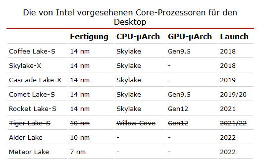
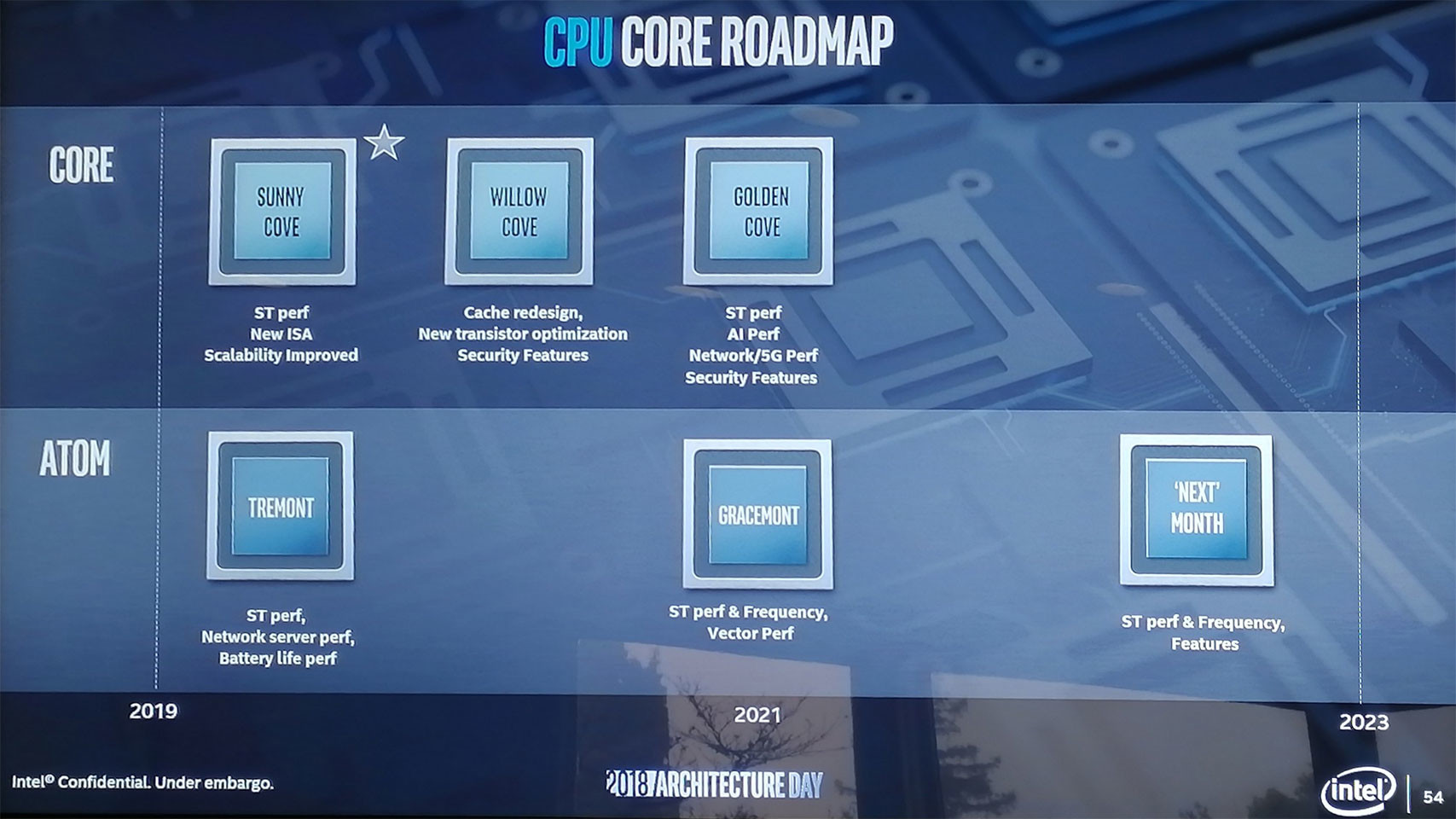
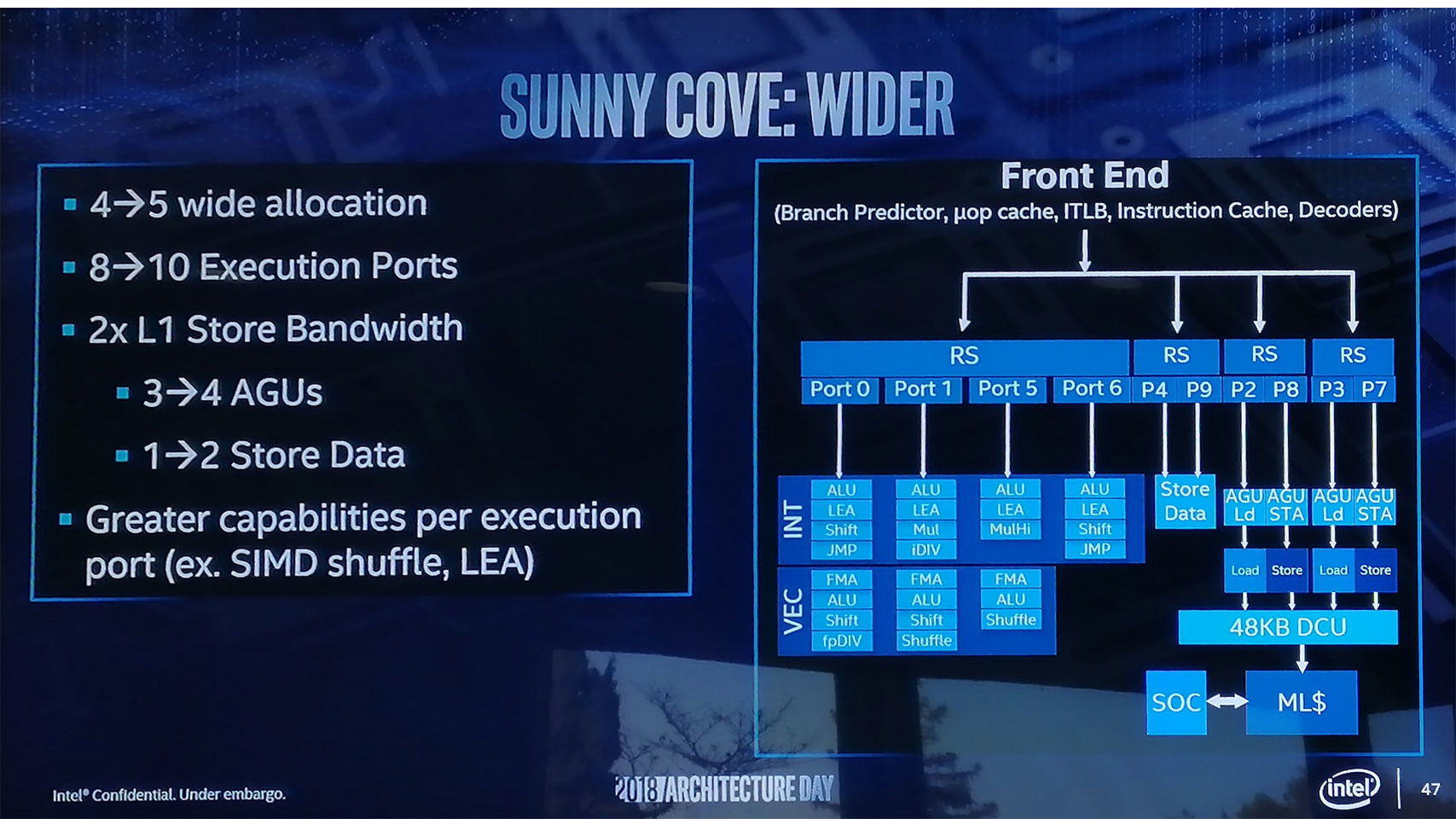
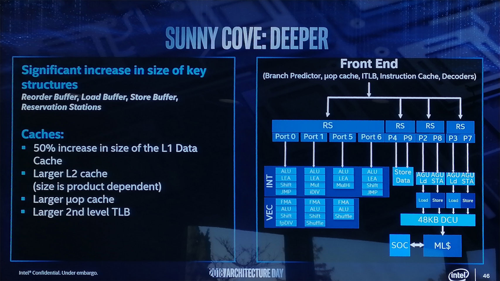
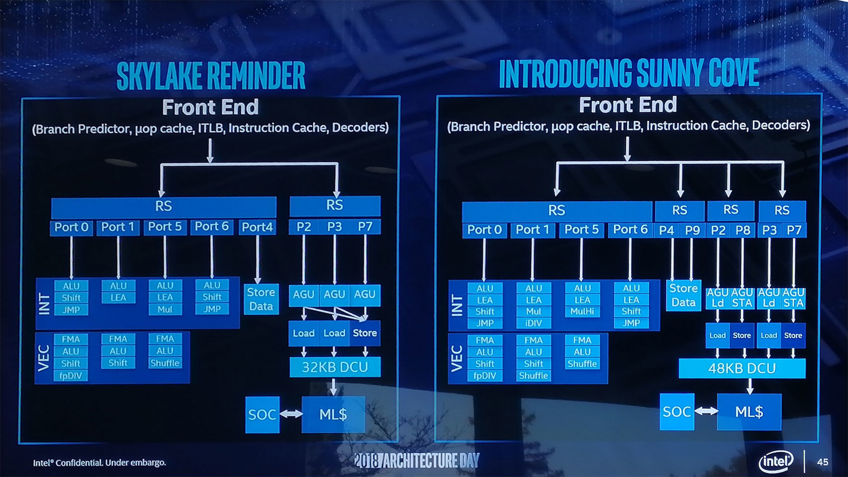
Huawei Reportedly Develops Chip Design Tools for 14 nm and Above

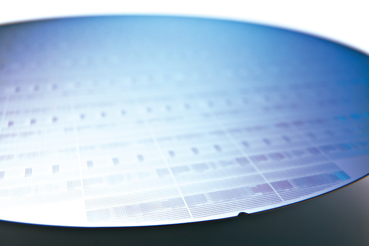
Amid the US sanctions, Chinese technology giant Huawei has reportedly developed tools to create processors with 14 nm and above lithography. According to Chinese media Yicai, Huawei and its semiconductor partners have teamed up to create replacement tools in place of US chip toolmakers like Cadence, Synopsys, and Mentor/Siemens. These three companies control all of the world's Electronic Design Automation (EDA) tools used for every step of chip design, from architecture to placement and routing to the final physical layout. Many steps need to be taken before making a tapeout of a physical chip, and Huawei's newly developed EDA tools will help the Chinese industry with US sanctions which crippled Huawei for a long time.

Having no access to US-made chipmaking tools, Huawei has invested substantial time into making these EDA tools. However, with competing EDA makers supporting lithography way below 14 nm, Huawei's job still needs to be completed. Chinese semiconductor factories are currently capable of 7 nm chip production, and Huawei itself is working on making a sub-7 nm EUV scanner to aid manufacturing goals and compete with the latest from TSMC and other. If Huawei can create EUV scanners that can achieve transistor sizes smaller than 7 nm, we expect to see their EDA tools keep pace as well. It is only a matter of time before they announce adaptation for smaller nodes.

Intel "Meteor Lake" and "Arrow Lake" Use GPU Chiplets

Intel's upcoming "Meteor Lake" and "Arrow Lake" client mobile processors introduce an interesting twist to the chiplet concept. Earlier represented in vague-looking IP blocks, new artistic impressions of the chip put out by Intel shed light on a 3-die approach not unlike the Ryzen "Vermeer" MCM that has up to two CPU core dies (CCDs) talking to a cIOD (client IO die), which handles all the SoC connectivity; Intel's design has one major difference, and that's integrated graphics. Apparently, Intel's MCM uses a GPU die sitting next to the CPU core die, and the I/O (SoC) die. Intel likes to call its chiplets "tiles," and so we'll go with that.

The Graphics tile, CPU tile, and the SoC or I/O tile, are built on three different silicon fabrication process nodes based on the degree of need for the newer process node. The nodes used are Intel 4 (optically 7 nm EUV, but with characteristics of a 5 nm-class node); Intel 20A (characteristics of 2 nm), and external TSMC N3 (3 nm) node. At this point we don't know which tile gets what. From the looks of it, the CPU tile has a hybrid CPU core architecture made up of "Redwood Cove" P-cores, and "Crestmont" E-core clusters.

Intel Rebadges 10nm Enhanced SuperFin Node as "Intel 7," Invents Other Creative Node Names

Intel, in a move comparable to its competitors' Performance Rating system from the 1990s, has invented a new naming scheme for its in-house foundry nodes to claim technological parity with contemporaries such as TSMC and Samsung, that are well into the sub-10 nm class. Back in the i586 era, when Intel's competitors such as AMD and Cyrix, couldn't keep up with its clock-speeds yet found their chips to be somewhat competitive, they invented the PR (processor rating) system, with a logical number attempting to denote parity with an Intel processor's clock-speed. For example, a PR400 processor rating meant that the chip rivaled a Pentium II 400 MHz (which it mostly didn't). The last that the PR system made sense was with the final generation of single-core performance chips, Pentium 4 and Athlon XP, beyond which, the introduction of multi-core obfuscated the PR system. A Phenom X4 9600 processor didn't mean performance on par with a rival Intel chip running at an impossible 9.60 GHz.

Intel's new foundry naming system sees its 10 nm Enhanced SuperFin node re-badge as "Intel 7." The company currently builds 11th Gen Core "Tiger Lake" processors on the 10 nm SuperFin node, and is expected to build its upcoming 12th Gen Core "Alder Lake" chips on its refinement, the 10 nm Enhanced SuperFin, which will now be referred to as "Intel 7." The company is careful to avoid using the nanometer unit next to the number, instead signaling the consumer that the node somehow offers transistor density and power characteristics comparable to a 7 nm node. Intel 7 offers a 10-15 percent performance/Watt gain over 10 nm SuperFin, and is already in volume production, with a debut within 2021 with "Alder Lake."

NVIDIA RTX 3080 Ti and GA102 "Ampere" Specs, Other Juicy Bits Revealed

PC hardware focused YouTube channel Moore's Law is Dead published a juicy tech-spec reveal of NVIDIA's next-generation "Ampere" based flagship consumer graphics card, the GeForce RTX 3080 Ti, citing correspondence with sources within NVIDIA. The report talks of big changes to NVIDIA's Founders Edition (reference) board design, as well as what's on the silicon. To begin with, the RTX 3080 Ti reference-design card features a triple-fan cooling solution unlike the RTX 20-series. This cooler is reportedly quieter than the RTX 2080 Ti FE cooling solution. The card pulls power from a pair of 8-pin PCIe power connectors. Display outputs include three DP, and one each of HDMI and VirtualLink USB-C. The source confirms that "Ampere" will implement PCI-Express gen 4.0 x16 host interface.

With "Ampere," NVIDIA is developing three tiers of high-end GPUs, with the "GA102" leading the pack and succeeding the "TU102," the "GA104" holding the upper-performance segment and succeeding today's "TU104," but a new silicon between the two, codenamed "GA103," with no predecessor from the current-generation. The "GA102" reportedly features 5,376 "Ampere" CUDA cores (up to 10% higher IPC than "Turing"). The silicon also taps into the rumored 7 nm-class silicon fabrication node to dial up GPU clock speeds well above 2.20 GHz even for the "GA102." Smaller chips in the series can boost beyond 2.50 GHz, according to the report. Even with the "GA102" being slightly cut-down for the RTX 3080 Ti, the silicon could end up with FP32 compute performance in excess of 21 TFLOPs. The card uses faster 18 Gbps GDDR6 memory, ending up with 863 GB/s of memory bandwidth that's 40% higher than that of the RTX 2080 Ti (if the memory bus width ends up 384-bit). Below are screengrabs from the Moore's Law is Dead video presentation, and not NVIDIA slides.

AMD Sheds Light on the Missing "+" in "7nm" for Zen 3 and RDNA2 in its Latest Presentation

AMD at its Financial Analyst Day 2020 presentation made a major clarification about its silicon fabrication process. It was previously believed that the company's upcoming "Zen 3" CPU microarchitecture and RDNA2 graphics architectures were based on TSMC's N7+ (7 nm EUV) silicon fabrication process because AMD would mark the two as "7 nm+" in its marketing slides. Throughout its Financial Analyst Day presentation, however, AMD avoided using that marker, and resorted to an amorphous "7 nm" marker, prompting one of the financial analysts to seek a clarification. At the time, AMD responded that they were aligning their marketing with that of TSMC, and hence chose to use "7 nm" in its new slides.

It turns out that the next step to TSMC N7, the company's current-generation 7 nm DUV silicon fabrication node, isn't N7+ (7 nm EUV), but rather it has a nodelet along the way, which the foundry refers to as N7P. This is a generational refinement of N7, but does not use EUV lithography, which means it may not offer the 15-20 percent gains in transistor densities offered by N7+ over N7. AMD clarified that "7 nm+" in its past presentations did not intend to signify N7+, and that the "+" merely denoted an improvement over N7. At the same time, it won't specify whether "Zen 3" and RDNA2 are based on N7P or N7+, so the company doesn't rule out N7+, either. We'll probably learn more as we near the late-2020 launch of "Zen 3" as EPYC "Milan."
AMD CPU Roadmap Zen 3 Zen 4 AMD CPU Roadmap Zen 2 Zen 3

AMD "Zen 4" Microarchitecture On Track for 2021-22 Debut with "Genoa"

AMD's 4th generation EPYC line of enterprise processors, now into design stage, impressed the United States Department of Energy enough that it wants to deploy it in "El Capitan," a 2 ExaFLOP supercomputer that will be the world's most powerful, when it goes online around 2022. Codenamed "Genoa," 4th gen EPYC implements AMD's "Zen 4" microarchitecture. While AMD didn't get into too many details about it in its 2020 Financial Analyst Day address, there are a couple of details.

For starters, "Zen 4" continues on AMD's trajectory of adding IPC gains with each generation. Secondly, "Zen 4" will leverage the advanced 5 nm silicon fabrication process, which should significantly increase transistor densities over even the most advanced iterations of 7 nm, such as 7 nm EUV. "Zen 4" comes out roughly the same time as the RDNA3 and CDNA2 graphics architectures, and AMD's 3rd generation Infinity Fabric interconnect that enables exascale supercomputers thanks to coherent unified memory and vast shared memory pools between CPUs and compute GPUs. Elsewhere in the roadmap, we see AMD announcing that its upcoming "Zen 3" microarchitecture and its enterprise implementation, the EPYC "Milan" processor, will release only toward the end of 2020. This would give EPYC "Rome" close to 6 calendar quarters of market leadership.

AMD RDNA2 Graphics Architecture Detailed, Offers +50% Perf-per-Watt over RDNA

With its 7 nm RDNA architecture that debuted in July 2019, AMD achieved a nearly 50% gain in performance/Watt over the previous "Vega" architecture. At its 2020 Financial Analyst Day event, AMD made a big disclosure: that its upcoming RDNA2 architecture will offer a similar 50% performance/Watt jump over RDNA. The new RDNA2 graphics architecture is expected to leverage 7 nm+ (7 nm EUV), which offers up to 18% transistor-density increase over 7 nm DUV, among other process-level improvements. AMD could tap into this to increase price-performance by serving up more compute units at existing price-points, running at higher clock speeds.

AMD has two key design goals with RDNA2 that helps it close the feature-set gap with NVIDIA: real-time ray-tracing, and variable-rate shading, both of which have been standardized by Microsoft under DirectX 12 DXR and VRS APIs. AMD announced that RDNA2 will feature dedicated ray-tracing hardware on die. On the software side, the hardware will leverage industry-standard DXR 1.1 API. The company is supplying RDNA2 to next-generation game console manufacturers such as Sony and Microsoft, so it's highly likely that AMD's approach to standardized ray-tracing will have more takers than NVIDIA's RTX ecosystem that tops up DXR feature-sets with its own RTX feature-set.
AMD GPU Architecture Roadmap RDNA2 RDNA3 AMD RDNA2 Efficiency Roadmap AMD RDNA2 Performance per Watt AMD RDNA2 Raytracing

AMD Announces the CDNA and CDNA2 Compute GPU Architectures

AMD at its 2020 Financial Analyst Day event unveiled its upcoming CDNA GPU-based compute accelerator architecture. CDNA will complement the company's graphics-oriented RDNA architecture. While RDNA powers the company's Radeon Pro and Radeon RX client- and enterprise graphics products, CDNA will power compute accelerators such as Radeon Instinct, etc. AMD is having to fork its graphics IP to RDNA and CDNA due to what it described as market-based product differentiation.

Data centers and HPCs using Radeon Instinct accelerators have no use for the GPU's actual graphics rendering capabilities. And so, at a silicon level, AMD is removing the raster graphics hardware, the display and multimedia engines, and other associated components that otherwise take up significant amounts of die area. In their place, AMD is adding fixed-function tensor compute hardware, similar to the tensor cores on certain NVIDIA GPUs.
AMD Datacenter GPU Roadmap CDNA CDNA2 AMD CDNA Architecture AMD Exascale Supercomputer

AMD Radeon Instinct MI100 "Arcturus" Hits the Radar, We Have its BIOS

AMD's upcoming large post-Navi graphics chip, codenamed "Arcturus," will debut as "Radeon Instinct MI100", which is an AI-ML accelerator under the Radeon Instinct brand, which AMD calls "Server Accelerators." TechPowerUp accessed its BIOS, which is now up on our VGA BIOS database. The card goes with the device ID "0x1002 0x738C," which confirms "AMD" and "Arcturus,". The BIOS also confirms that memory size is at a massive 32 GB HBM2, clocked at 1000 MHz real (possibly 1 TB/s bandwidth, if memory bus width is 4096-bit).

Both Samsung (KHA884901X) and Hynix memory (H5VR64ESA8H) is supported, which is an important capability for AMD's supply chain. From the ID string "MI100 D34303 A1 XL 200W 32GB 1000m" we can derive that the TDP limit is set to a surprisingly low 200 W, especially considering this is a 128 CU / 8,192 shader count design. Vega 64 and Radeon Instinct MI60 for comparison have around 300 W power budget with 4,096 shaders, 5700 XT has 225 W with 2560 shaders, so either AMD achieved some monumental efficiency improvements with Arcturus or the whole design is intentionally running constrained, so that AMD doesn't reveal their hand to these partners, doing early testing of the card.

AMD to Outpace Apple as TSMC's Biggest 7nm Customer in 2020

AMD in the second half of 2020 could outpace Apple as the biggest foundry customer of TSMC for its 7 nm silicon fabrication nodes (DUV and EUV combined). There are two key factors contributing to this: AMD significantly increasing its orders for the year; and Apple transitioning to TSMC's 5 nm node for its A14 SoC, freeing up some 7 nm allocation, which AMD grabbed. AMD is currently tapping into 7 nm DUV for its "Zen 2" chiplet, "Navi 10," and "Navi 14" GPU dies. The company could continue to order 7 nm DUV until these products reach EOL; while also introducing the new "Renoir" APU die on the process. The foundry's new 7 nm+ (EUV) node will be utilized for "Zen 3" chiplets and "Navi 2#" GPU dies in 2020.

Currently, the top-5 customers for TSMC 7 nm are Apple, HiSilicon, Qualcomm, AMD, and MediaTek. Barring AMD, the others in the top-5 build mobile SoCs or 4G/5G modem chips on the node. AMD is expected to top the list as it scales up orders with TSMC. In the first half of 2020, TSMC's monthly output for 7 nm is expected to grow to 110,000 wafers per month (wpm). Apple's migration to 5 nm in 2H-2020, coupled with capacity-addition could take TSMC's 7 nm output to 140,000 wpm. AMD has reportedly booked the entire capacity-addition for 30,000 wpm, taking its allocation up to 21% in 2H-2020. Qualcomm is switching to Samsung for its next-generation SoCs and modems designed for 7 nm EUV. NVIDIA, too, is expected to built its next-gen 7 nm EUV GPUs on Samsung instead of TSMC. These moves by big players could free up significant foundry allocation at TSMC for AMD's volumes to grow in 2020.

AMD CEO To Unveil "Zen 3" Microarchitecture at CES 2020

A prominent Taiwanese newspaper reported that AMD will formally unveil its next-generation "Zen 3" CPU microarchitecture at the 2020 International CES. Company CEO Dr Lisa Su will head an address revealing three key client-segment products under the new 4th generation Ryzen processor family, and the company's 3rd generation EPYC enterprise processor family based on the "Milan" MCM that succeeds "Rome." AMD is keen on developing an HEDT version of "Milan" for the 4th generation Ryzen Threadripper family, codenamed "Genesis Peak."

The bulk of the client-segment will be addressed by two distinct developments, "Vermeer" and "Renoir." The "Vermeer" processor is a client-desktop MCM that succeeds "Matisse," and will implement "Zen 3" chiplets. "Renoir," on the other hand, is expected to be a monolithic APU that combines "Zen 2" CPU cores with an iGPU based on the "Vega" graphics architecture, with updated display- and multimedia-engines from "Navi." The common thread between "Milan," "Genesis Peak," and "Vermeer" is the "Zen 3" chiplet, which AMD will build on the new 7 nm EUV silicon fabrication process at TSMC. AMD stated that "Zen 3" will have IPC increases in line with a new microarchitecture.

Ray Tracing and Variable-Rate Shading Design Goals for AMD RDNA2

Hardware-accelerated ray tracing and variable-rate shading will be the design focal points for AMD's next-generation RDNA2 graphics architecture. Microsoft's reveal of its Xbox Series X console attributed both features to AMD's "next generation RDNA" architecture (which logically happens to be RDNA2). The Xbox Series X uses a semi-custom SoC that features CPU cores based on the "Zen 2" microarchitecture and a GPU based on RDNA2. It's highly likely that the SoC could be fabricated on TSMC's 7 nm EUV node, as the RDNA2 graphics architecture is optimized for that. This would mean an optical shrink of "Zen 2" to 7 nm EUV. Besides the SoC that powers Xbox Series X, AMD is expected to leverage 7 nm EUV for its RDNA2 discrete GPUs and CPU chiplets based on its "Zen 3" microarchitecture in 2020.

Variable-rate shading (VRS) is an API-level feature that lets GPUs conserve resources by shading certain areas of a scene at a lower rate than the other, without perceptible difference to the viewer. Microsoft developed two tiers of VRS for its DirectX 12 API, tier-1 is currently supported by NVIDIA "Turing" and Intel Gen11 architectures, while tier-2 is supported by "Turing." The current RDNA architecture doesn't support either tiers. Hardware-accelerated ray-tracing is the cornerstone of NVIDIA's "Turing" RTX 20-series graphics cards, and AMD is catching up to it. Microsoft already standardized it on the software-side with the DXR (DirectX Raytracing) API. A combination of VRS and dynamic render-resolution will be crucial for next-gen consoles to achieve playability at 4K, and to even boast of being 8K-capable.

AMD "Zen 4" 2021 Launch On Track as TSMC Optimistic About 5 nm

AMD's "Zen 4" CPU microarchitecture is on track for a 2021 launch as its principal foundry partner, TSMC, is optimistic about early yields of its 5 nm silicon fabrication node. TSMC supports the 5 nm product roadmaps of not just AMD, but also Apple and HiSilicon. "Zen 4" is particularly important for AMD, as it will release its next enterprise platform, codenamed "Genoa," along with the new SP5 socket. The new socket will present AMD with the opportunity to significantly change the processor's I/O, such as support for a new memory standard, a new PCIe generation, more memory channels, more PCIe lanes, etc. As early as 2019, the foundry is seeing yields of over 50 percent for the 5 nm node (possibly risk production designed to test the node), which is very encouraging for its customers.

AMD's roadmap for 2020 sees the introduction of "Zen 3" on the 7 nm EUV process (dubbed 7 nm+). AMD recently commented that the performance uplift of "Zen 3" versus "Zen 2" will be "right in line with what you would expect from an entirely new architecture." The 7 nm EUV node provides a significant 20 percent increase in transistor-density compared to the current 7 nm DUV node "Zen 2" chiplets and the company's "Navi" family of GPUs are built on. "Zen 3" could see the company do away with the CCX (quad-core CPU complex), and make chiplets monolithic blocks of CPU cores without sub-divisions. For the client-segment, 5 is a recurring number in 2021. It will see the introduction of the 5th generation Ryzen processors (5000-series), built on the 5 nm process, supporting DDR5 memory, PCI-Express gen 5, and the new AM5 client-segment CPU socket.

AMD "Zen 3" Microarchitecture Could Post Significant Performance Gains

At its recent SC19 talk, AMD touched upon its upcoming "Zen 3" CPU microarchitecture. Designed for the 7 nm EUV silicon fabrication process that significantly increases transistor densities, "Zen 3" could post performance gains "right in line with what you would expect from an entirely new architecture," states AMD, referring to the roughly 15 percent IPC gains that were expected of "Zen 2" prior to its launch. "Zen 2" IPC ended up slightly over 15 percent higher than that of the original "Zen" microarchitecture. AMD's SC19 comments need not be a guidance on the IPC itself, but rather performance gains of end-products versus their predecessors.

The 7 nm EUV process, with its 20 percent transistor-density increase could give AMD designers significant headroom to increase clock speeds to meet the company's generational performance improvement targets. Another direction in which "Zen 3" could go is utilizing the additional transistor density to bolster its core components to support demanding instruction-sets such as AVX-512. The company's microarchitecture is also missing something analogous to Intel's DLBoost, an instruction-set that leverages fixed-function hardware to accelerate AI-DNN building and training. Even VIA announced an x86 microarchitecture with AI hardware and AVX-512 support. In either case, the design of "Zen 3" is complete. We'll have to wait until 2020 to find out how fast "Zen 3" is, and the route taken to get there.

Intel Scraps 10nm for Desktop, Brazen it Out with 14nm Skylake Till 2022?

In a shocking piece of news, Intel has reportedly scrapped plans to launch its 10 nm "Ice Lake" microarchitecture on the client desktop platform. The company will confine its 10 nm microarchitectures, "Ice Lake" and "Tiger Lake" to only the mobile platform, while the desktop platform will see derivatives of "Skylake" hold Intel's fort under the year 2022! Intel gambles that with HyperThreading enabled across the board and increased clock-speeds, it can restore competitiveness with AMD's 7 nm "Zen 2" Ryzen processors with its "Comet Lake" silicon that offers core-counts of up to 10.

"Comet Lake" will be succeeded in 2021 by the 14 nm "Rocket Lake" silicon, which somehow combines a Gen12 iGPU with "Skylake" derived CPU cores, and possibly increased core-counts and clock speeds over "Comet Lake." It's only 2022 that Intel will ship out a truly new microarchitecture on the desktop platform, with "Meteor Lake." This chip will be built on Intel's swanky 7 nm EUV silicon fabrication node, and possibly integrate CPU cores more advanced than even "Willow Cove," possibly "Golden Cove."

Intel's Gargantuan Next-gen Enterprise CPU Socket is LGA4677

Intel has finalized design of its next-generation Xeon Scalable enterprise CPU socket for its "Sapphire Rapids" processors. Called LGA4677, the socket succeeds LGA3647, and is bound for a 2021 market release. Intel will have transitioned to its advanced 7 nm EUV silicon fabrication node on the CPU front, and has adopted an "enterprise-first" strategy for the node. LGA4677 will be designed to handle the extremely high bandwidth of PCI-Express Gen 5, which doubles bandwidth over PCIe gen 4.0, and adds several enterprise-specific features Intel is rolling out in advance as part of its CXL interconnect. These details, along with a prototype LGA4189 socket, was revealed at an exhibit by TE Connectivity, a company that manufactures the socket. The additional pin-count could enable Intel to not just deploy PCI-Express Gen 5, but also expand I/O in other directions, such as more memory channels, dedicated Persistent Memory I/O, etc.

AMD Zen 3 Could Bid the CCX Farewell, Feature Updated SMT

With its next-generation "Zen 3" CPU microarchitecture designed for the 7 nm EUV silicon fabrication process, AMD could bid the "Zen" compute complex or CCX farewell, heralding chiplets with monolithic last-level caches (L3 caches) that are shared across all cores on the chiplet. AMD embraced a quad-core compute complex approach to building multi-core processors with "Zen." At the time, the 8-core "Zeppelin" die featured two CCX with four cores, each. With "Zen 2," AMD reduced the CPU chiplet to only containing CPU cores, L3 cache, and an Infinity Fabric interface, talking to an I/O controller die elsewhere on the processor package. This reduces the economic or technical utility in retaining the CCX topology, which limits the amount of L3 cache individual cores can access.

This and more juicy details about "Zen 3" were put out by a leaked (later deleted) technical presentation by company CTO Mark Papermaster. On the EPYC side of things, AMD's design efforts will be spearheaded by the "Milan" multi-chip module, featuring up to 64 cores spread across eight 8-core chiplets. Papermaster talked about how the individual chiplets will feature "unified" 32 MB of last-level cache, which means a deprecation of the CCX topology. He also detailed an updated SMT implementation that doubles the number of logical processors per physical core. The I/O interface of "Milan" will retain PCI-Express gen 4.0 and eight-channel DDR4 memory interface.

AMD Readies the Low-Power "Dali" APU for Thin-and-Light Notebooks

AMD is expected to bring back its low-power APU family in 2020 with the new "Dali" silicon. Updated company roadmap slides see the inclusion of "Dali" as a "value mobile APU," positioned under "Renoir," a performance APU targeting both the mainstream notebook and desktop (socket AM4) platforms. AMD looks keen to branch out its APU business in two directions.

"Renoir" is expected to be a "Zen 2" based APU with CPU performance matching at least the Ryzen 5 3600 or 3700X, and a faster "Vega" based iGPU. It wouldn't surprise us if "Dali" is a monolithic 7 nm die with two "Zen 2" CPU cores and a tiny iGPU with 3-4 compute units. "Renoir," on the other hand, could be an MCM with an 8-core "Zen 2" chiplet and an enlarged I/O controller die that has the iGPU. "Dali" could see the light of the day only in 2020, by which time TSMC could substantially increase its 7 nm volumes and clear the decks for its new 7 nm EUV mass-production.

Intel Switches Gears to 7nm Post 10nm, First Node Live in 2021

Intel's semiconductor manufacturing business has had a terrible past 5 years as it struggled to execute its 10 nanometer roadmap forcing the company's processor designers to re-hash the "Skylake" microarchitecture for 5 generations of Core processors, including the upcoming "Comet Lake." Its truly next-generation microarchitecture, codenamed "Ice Lake," which features a new CPU core design called "Sunny Cove," comes out toward the end of 2019, with desktop rollouts expected 2020. It turns out that the 10 nm process it's designed for, will have a rather short reign at Intel's fabs. Speaking at an investor's summit on Wednesday, Intel put out its silicon fabrication roadmap that sees an accelerated roll-out of Intel's own 7 nm process.

When it goes live and fit for mass production some time in 2021, Intel's 7 nm process will be a staggering 3 years behind TSMC, which fired up its 7 nm node in 2018. AMD is already mass-producing CPUs and GPUs on this node. Unlike TSMC, Intel will implement EUV (extreme ultraviolet) lithography straightaway. TSMC began 7 nm with DUV (deep ultraviolet) in 2018, and its EUV node went live in March. Samsung's 7 nm EUV node went up last October. Intel's roadmap doesn't show a leap from its current 10 nm node to 7 nm EUV, though. Intel will refine the 10 nm node to squeeze out energy-efficiency, with a refreshed 10 nm+ node that goes live some time in 2020.

China-based SMIC to Start Manufacture of 14 nm-class Chips in 2H 2019

As R&D costs for new, smaller manufacturing nodes grow at unprecedented rates across the industry, a new player is set to enter the 14 nm process manufacture competition: China-based SMIC (Semiconductor Manufacturing International Corporation). The company is looking to throw its hat on the lucrative 14 nm process, filling its offerings portfolio under the 28 nm it currently offers as its denser process.

The company expects its 95% yield rate to offer its customers a trusted platform that might help it increase revenue for further investment on its 10 nm and 7 nm EUV nodes, which the company is pursuing (despite other industry veterans, such as former AMD-manufacturing arm GLOBALFOUNDRIES having ceased development on). Manufacturing technology that's competitive with the western world's, and that's developed in-country, is paramount for China's intention of reducing its dependence of foreign technology, which is why this is such a big step for the company and the company's aspirations.

TSMC 7nm EUV Process to Enter Mass-Production in March 2019

TSMC is giving final touches to set its flagship 7 nanometer EUV (extreme ultraviolet lithography) silicon fabrication node at its highest state of readiness for business, called mass-production. At this state, the node can mass-produce products for TSMC's customers. TSMC had taped out its first 7 nm EUV chips in October 2018. The company will also begin risk-production of the more advanced 5 nm node in April, staying on schedule. Mass production of 5 nm chips could commence in the first half of 2020.

The 7 nm EUV node augments TSMC's 7 nm DUV (deep ultraviolet lithography) node that's been already active since April 2018, and producing chips for AMD, Apple, HiSilicon, and Xilinx. At the turn of the year, 7 nm DUV made up 9 percent of TSMC's shipments. With the new node going online, 7 nm (DUV + EUV) could make up 25 percent of TSMC's output by the end of 2019.

NVIDIA to Implement 7nm EUV Node for its 2020 GPUs

NVIDIA will implement the 7 nanometer EUV (extreme ultraviolet) lithography to build its future generation of GPUs slated for 2020, according to Japanese publication MyNavi.jp. The GPU giant could be among the first customers besides IBM, to contract Samsung for 7 nm EUV mass-production of GPUs. IBM will use the Korean semiconductor giant for manufacturing Z-series processors and FPGAs. Samsung announced in October 2018 that it will begin risk-production on its 7 nm EUV node in early-2019.

An earlier report from 2018 also forecast NVIDIA implementing 7 nm DUV (deep ultraviolet) node of TSMC for its 2019 GPU lineup. With news of the company now working with Samsung on 7 nm EUV for 2020, this seems less likely. It's possible that NVIDIA could somehow split its next generation GPU lineup between TSMC 7 nm DUV and Samsung 7 nm EUV, with the latter being used for chips with higher transistor-counts, taking advantage of the node's higher deliverable transistor densities.

IBM Expands Strategic Partnership with Samsung to Include 7nm Chip Manufacturing

IBM today announced an agreement with Samsung to manufacture 7-nanometer (nm) microprocessors for IBM Power Systems , IBM Z and LinuxONE , high-performance computing (HPC) systems, and cloud offerings. The agreement combines Samsung's industry-leading semiconductor manufacturing with IBM's high-performance CPU designs. This combination is being designed to drive unmatched systems performance, including acceleration, memory and I/O bandwidth, encryption and compression speed, as well as system scaling. It positions IBM and Samsung as strategic partners leading the new era of high-performance computing specifically designed for AI.

"At IBM, our first priority is our clients," said John Acocella, Vice President of Enterprise Systems and Technology Development for IBM Systems. "IBM selected Samsung to build our next generation of microprocessors because they share our level of commitment to the performance, reliability, security, and innovation that will position our clients for continued success on the next generation of IBM hardware."

Intel Unveils a Clean-slate CPU Core Architecture Codenamed "Sunny Cove"

Intel today unveiled its first clean-slate CPU core micro-architecture since "Nehalem," codenamed "Sunny Cove." Over the past decade, the 9-odd generations of Core processors were based on incrementally refined descendants of "Nehalem," running all the way down to "Coffee Lake." Intel now wants a clean-slate core design, much like AMD "Zen" is a clean-slate compared to "Stars" or to a large extent even "Bulldozer." This allows Intel to introduce significant gains in IPC (single-thread performance) over the current generation. Intel's IPC growth curve over the past three micro-architectures has remained flat, and only grew single-digit percentages over the generations prior.

It's important to note here, that "Sunny Cove" is the codename for the core design. Intel's earlier codenaming was all-encompassing, covering not just cores, but also uncore, and entire dies. It's up to Intel's future chip-designers to design dies with many of these cores, a future-generation iGPU such as Gen11, and a next-generation uncore that probably integrates PCIe gen 4.0 and DDR5 memory. Intel details "Sunny Cove" as far as mentioning IPC gains, a new ISA (new instruction sets and hardware capabilities, including AVX-512), and improved scalability (ability to increase core-counts without running into latency problems).

Intel 7nm EUV Node Back On Track, 2x Transistor Densities Over 10nm

There could be light at the end of the tunnel for Intel's silicon fabrication business after all, as the company reported that its 7 nanometer silicon fabrication node, which incorporates EUV (extreme ultraviolet) lithography, is on track. The company stressed in its Nasdaq Investors' Conference presentation that its 7 nm EUV process is de-linked from its 10 nm DUV (deep ultraviolet) node, and that there are separate teams working on their development. The 10 nm DUV node is qualitatively online, and is manufacturing small batches of low-power mobile "Cannon Lake" Core processors.

Cannon Lake is an optical shrink of the "Skylake" architecture to the 10 nm node. Currently there's only one SKU based on it, the Core i3-8121U. Intel utilized the electrical gains from the optical shrink to redesign the client-segment architecture's FPU to support the AVX-512 instruction-set (although not as feature-rich as the company's enterprise-segment "Skylake" derivatives). The jump from 10 nm DUV to 7 nm EUV will present a leap in transistor densities, with Intel expecting nothing short of a doubling. 10 nm DUV uses a combination of 193 nm wavelength ultraviolet lasers and multi-patterning to achieve its transistor density gains over 14 nm++. The 7 nm EUV node uses an extremely advanced 135 nm indirect laser, reducing the need for multi-patterning. The same laser coupled with multi-patterning could be Intel's ticket to 5 nm.
Return to Keyword Browsing
Jun 1st, 2024 03:36 EDT change timezone

New Forum Posts

Popular Reviews

Controversial News Posts