News Posts matching #ASML

Return to Keyword Browsing

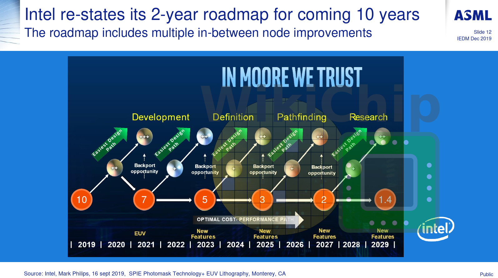
Intel's Process Roadmap Gets Updated with Plans to go Back to Two Year Cadence

During the IEDM event hosted by the IEEE organization, ASML's CEO, Martin van den Brink, took the stage to elaborate more on ASML's vision of the future of semiconductors. When talking about the future of semiconductors, Mr. Brink started talking about Intel and their vision for the future. Intel's slides were showing many things including backporting of IP to older processes and plan to go back to "tick-tock" two-year cadence to restore the previous confidence in Intel's manufacturing capabilities.

Perhaps one of the most interesting notes about the presentation is the fact that Intel is working hard to realize its plans of bringing back a two-year cadence of "tick-tock" process realization. That means that in the future, presumably after 10 nm debut problems are solved, Intel wants to do the old process and optimization tactics. A slide (shown below) titled "In Moore We Trust" is speaking a lot about Intel's future plans, showing few things in particular: Intel's upcoming 10 nm++ and 10 nm+++ nodes, and the possibility of backporting.

Challenges With 7 nm, 5 nm EUV Technologies Could Lead to Delays In Process' TTM

Semiconductor manufacturers have been historically bullish when it comes to the introduction of new manufacturing technologies. Intel, AMD (and then Globalfoundries), TSMC, all are companies who thrive in investors' confidence: they want to paint the prettiest picture they can in terms of advancements and research leadership, because that's what attracts investment, and increased share value, and thus, increased funds to actually reach those optimistic goals.

However, we've seen in recent years how mighty Intel itself has fallen prey to unforeseen complications when it comes to advancements of its manufacturing processes, which saw us go from a "tick-tock" cadence of new architecture - new manufacturing process, to the introduction of 14 nm ++ processes. And as Intel, Globalfoundries and TSMC race towards sub 7-nm manufacturing processes with 250 mm wafers and EUV usage, things aren't getting as rosy as the ultraviolet moniker would make us believe.

Q4 2017 300 mm Silicon Wafer Pricing to Increase 20% YoY in DRAM-like Squeeze

Silicon wafers are definitely the best kind of wafers for us tech enthusiasts, but as we all know, required financial resources for the development and production of these is among the most intensive in development costs and R&D. It's not just about the cost of employing enough (and crucially, good enough) engineers that can employ the right tools and knowledge to design the processing miracles that are etched onto wafers; there's also the cost of good, old production as well. Extreme Ultraviolet Lithography Systems that are used for the production of silicon wafers are about the size of a city bus, and typically cost more than 100 million euros ($115.3 million) each. ASML, a Dutch company that specializes in this kind of equipment, announced this year it was expecting to see a 25% revenue growth for 2017. Increased demand for these systems - and added cost of development of ever increasingly small and complex etchings in wafers - means this sector is seeing strong growth. But where there is strong growth, there is usually high demand, and high demand means higher strain on supply, which may sometimes not be able to keep up with the market's needs.

This is seemingly the case for wafer pricing; as demand for wafer production has been increasing, so to are prices. Faced with increased demand, companies are usually faced with a tough question to answer in regards to the correct course of action. Usually, it goes like this: higher demand at the same supply level means higher pricing. However, if supply isn't enough to satisfy demand, manufacturers are losing out on potential increased sales. This leads most companies to increase supply relative to demand, but always with lower projected output than demand requires, so they can bask in both increased ASP (Average Sale Price) and higher number of sales. This has been the case with DRAM memory production for some time now: and is happening with 300 mm silicon wafers as well.

TSMC to Build World's First 3 nm Fab in Taiwan

TSMC has announced the location for their first 3 nm fab: it will be built in the Tainan Science Park, southern Taiwan. Rumors pegged the new 3 nm factory as possibly being built in the US, due to political reasons; however, TSMC opted to keep their production capabilities clustered in the Tainan Science Park, where they can better leverage their assets and supply chain for the production and support of the world's first 3 nm semiconductor factory. It certainly also helped the Taiwanese government's decision to pledge land, water, electricity and environmental protection support to facilitate TSMC's latest manufacturing plan. It's expected that at least part of the manufacturing machines will be provided by ASML, a Netherlands-based company which has enjoyed 25% revenue growth already just this year.

As part of the announcement, TSMC hasn't given any revised timelines for their 3 nm production, which likely means the company still expects to start 3 nm production by 2022. TSMC said its 7 nm yield is ahead of schedule, and that it expects a fast ramp in 2018 - which is interesting, considering the company has announced plans to insert several extreme ultraviolet (EUV) layers at 7 nm. TSMC has also said its 5 nm roadmap is on track for a launch in the first quarter of 2019.

Demand for EUV Fabrication Systems Increasing; ASML Sees 25% Revenue Growth

Dutch company ASML may not be very known to us mortal users, but it has one of the greatest aces up its sleeve: it specializes in what are some of the most complex machines currently made by mankind. Extreme Ultraviolet Lithography Systems (EUV) are the kind of machines that make you look in wonder and amazement at man's ingenuity - ASML, which specializes in this type of systems, has a production capability for 2017 that numbers just 12 of these. That means on average, they take a whole month putting one of these together. That really goes to show the complexity inherent to these systems. And it shows: EUV machines are about the size of a city bus, and typically cost more than 100 million euros ($115.3 million) each.

The revenue growth forecast is spurred by an additional 8 EUV systems being ordered by ASML's clients, which include Intel, Samsung, and TSMC - some of the biggest players in the semiconductor business. The new orders brought the company's order backlog to 27 machines - more than double their current annual output. ASML is taking steps to to ensure an increase in production capability to keep up with the multi million-dollar demand: the company is set to expand its system production capability to 24 in 2018, before reaching an expected capacity of around 40 systems in 2019. Third-quarter revenue will be about 2.2 billion euros ($2.5 billion), the Veldhoven, Netherlands-based maker of chip-making machines predicts. The company's stock valuation has increased some 30% over the past year - the company's valuation currently stands at around €53 billion ($61 billion.)
Return to Keyword Browsing
May 21st, 2024 10:02 EDT change timezone

New Forum Posts

Popular Reviews

Controversial News Posts