News Posts matching #Alder Lake

Return to Keyword Browsing

Intel's Secret Sauce at Catching Up with AMD Core Count is the Gracemont E-core and its Mind-boggling Perf/Watt

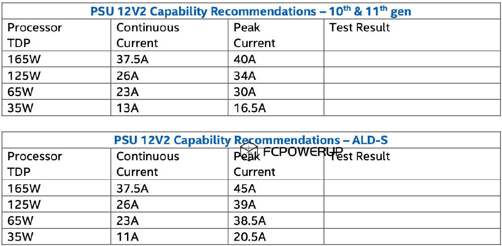
When early benchmarks of the Core i9-12900K "Alder Lake-S" processor showing performance comparable to AMD's top 16-core Ryzen 9 5950X surfaced, we knew something was up. 8 Intel P-cores and 8 E-cores, are able to match 16 "Zen 3" cores that are all performance cores. Apparently Intel is able to turn its P-core deficit around by taking a wacky approach. First, the 8 "Golden Cove" P-cores themselves offer significantly higher IPC than "Zen 3." Second, the 8 "Gracemont" E-cores aren't as "slow" as conventional wisdom would suggest.

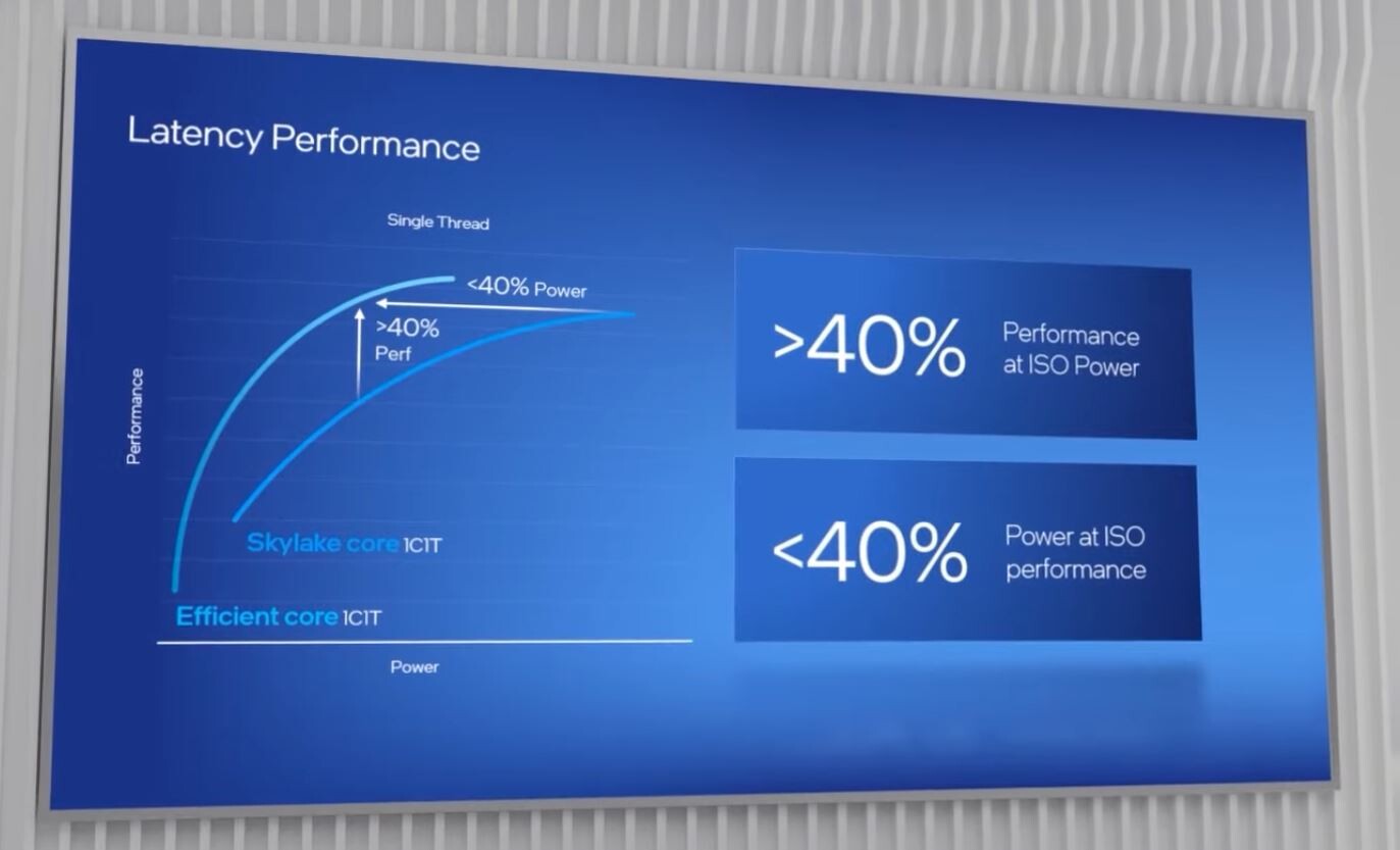
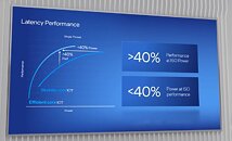
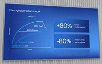
Intel in its Architecture Day presentation put out some astounding numbers that help support how 8 big + 8 little cores are able to perform in the league of 16 AMD big cores. Apparently, on "Alder Lake-S," the 8 "Gracemont" E-cores enjoy a lavish power budget, and are able to strike an incredible performance/Watt sweet-spot. Intel claims that the "Gracemont" E-core offers 40% higher performance at ISO power than a "Skylake" core (Intel's workhorse P-core for desktops until as recently as 2020); which means it consumes 40% less power at comparable performance.

Intel "Alder Lake" Silicon Variants Detailed—Reunification of the Product Lines

The 12th Gen Core "Alder Lake" microarchitecture will see Intel unify its desktop- and mobile processor IP, back to the way things were up to the 9th Gen. With its post-14 nm silicon fabrication nodes in their infancy, Intel had diverged the client processor IP across its 10th and 11th Gen Core. With 10th Gen, the company introduced "Ice Lake" for ultra-portable platforms (28 W and below), while retaining 14 nm "Comet Lake" for mainstream notebooks (28 W to 45 W); while keeping desktop exclusively with 14 nm "Comet Lake." For 11th Gen, the story is mostly similar. Cutting-edge 10 nm "Tiger Lake" now covers all mobile categories, while desktop receives an IPC upgrade, thanks to the 14 nm "Rocket Lake." The 12th Gen will see a common microarchitecture, "Alder Lake," span across all client segments, from 7 W ultra mobile, to 125 W enthusiast desktop.

This, however, doesn't mean that Intel has a one-size fits all silicon that it can carve SKUs out of. The company has developed as many as three physical dies based on "Alder Lake," which vary in CPU core counts, the size of the iGPU, and other on-die components. "Alder Lake" is a hybrid processor with a combination of larger "Golden Cove" P-cores, and smaller "Gracemont" E-cores. The P-cores are spatially large, and along with their L3 cache slices, take up a large share of the compute portion of the silicon. The E-cores come in clusters of 4 cores each.

Intel Thread Director Makes "Alder Lake" Hybrid Architecture Work

Intel in its Architecture Day presentation Thread Director, a hardware component present on the "Alder Lake" silicon, which makes the Hybrid architecture of the processor work flawlessly. "Alder Lake-S" is the first desktop processor with two kinds of x86 CPU cores—the larger Performance P-cores, and the smaller Efficient E-cores, which work in a setup not unlike big.LITTLE by Arm.

The x86-based "Alder Lake" processor has a much more complex ISA, and the E-cores don't have all of the instruction sets or hardware capabilities that the P-cores do. The two cores operate at very different performance/Watt bands, and are optimized for vastly different workloads. At the same time, sending a workload to the wrong kind of core could not only impact performance, but also crash, due to an ISA mismatch. Intel realized that it will take a lot more than mere OS-level awareness to solve the problem, and so innovated the Thread Director.

Intel Alder Lake ATX12V Peak Current Recommendation is Allegedly Higher Compared to Rocket Lake

Intel's upcoming Alder Lake family of processors, more specifically the desktop ALD-S SKUs, are supposedly going to require a higher peak current for the upcoming processors. In the table provided by the Chinese tech media outlet, FCPOWERUP, we are seeing that ALD-S processors have different power requirements for the ATX12V rails on their power supplies. The listed table shows the previous generation of Intel processors, the 10th and 11th generation, as available in 165 Watt variants. Even though there are no 165 Watt Comet Lake and Rocket Lake SKUs, this is only a placeholder for their PSU recommendations in case those SKUs were to be released.

According to the table, the peak current recommendation for the upcoming Alder Lake is higher at least 5 Amps across all SKUs. The 165 Watt SKUs have the requirement of 45 Amps (compared to the 40 A of Comet Lake and Rocket Lake), while the 125 Watt SKUs require 39 Amps, which is higher than the previous 34 Amp requirement. For 65 Watt models, the new peak recommendation is 38.5 Amps, a jump from the previous 30 Amp choice. The lowest rated 35 Watt SKUs are recommended to use 20.5 A, while the previous generations used 16.5 A current. It should be noted that the continuous rating has not been changed (new generation 35 Watt models actually use less current), which indicates that Alder Lake could have higher peak usages of power, meaning that PSU choice should be made with a 50-100 Watt higher rating.

Corsair Postulates That DDR5 Memory Runs Hotter

Corsair DIY Marketing Director, George Makris recently confirmed in a recent video that DDR5 memory could "conceivably could run much hotter than DDR4" due to voltage regulation being moved to the memory modules from the motherboard. This was reiterated by Corsair Memory Product Manager, Matt Woithe, who notes that they are prepared to handle this increased heat in Corsair DDR5 modules using their Dual-path Heat Xchange (DHX) technology. The next generation of memory also mandates the inclusion of on-die EEC which while not confirmed by Corsair will also add to the power budget of the modules. Corsair is expecting to release their first DDR5 memory modules towards the end of this year which will coincide with the launch of Intel's 12th Generation Alder Lake processors. AMD fans will need to wait until 2022 with the launch of Zen 4 to take advantage of the new DDR5 memory modules.

Intel Rebadges 10nm Enhanced SuperFin Node as "Intel 7," Invents Other Creative Node Names

Intel, in a move comparable to its competitors' Performance Rating system from the 1990s, has invented a new naming scheme for its in-house foundry nodes to claim technological parity with contemporaries such as TSMC and Samsung, that are well into the sub-10 nm class. Back in the i586 era, when Intel's competitors such as AMD and Cyrix, couldn't keep up with its clock-speeds yet found their chips to be somewhat competitive, they invented the PR (processor rating) system, with a logical number attempting to denote parity with an Intel processor's clock-speed. For example, a PR400 processor rating meant that the chip rivaled a Pentium II 400 MHz (which it mostly didn't). The last that the PR system made sense was with the final generation of single-core performance chips, Pentium 4 and Athlon XP, beyond which, the introduction of multi-core obfuscated the PR system. A Phenom X4 9600 processor didn't mean performance on par with a rival Intel chip running at an impossible 9.60 GHz.

Intel's new foundry naming system sees its 10 nm Enhanced SuperFin node re-badge as "Intel 7." The company currently builds 11th Gen Core "Tiger Lake" processors on the 10 nm SuperFin node, and is expected to build its upcoming 12th Gen Core "Alder Lake" chips on its refinement, the 10 nm Enhanced SuperFin, which will now be referred to as "Intel 7." The company is careful to avoid using the nanometer unit next to the number, instead signaling the consumer that the node somehow offers transistor density and power characteristics comparable to a 7 nm node. Intel 7 offers a 10-15 percent performance/Watt gain over 10 nm SuperFin, and is already in volume production, with a debut within 2021 with "Alder Lake."

Intel Accelerates Packaging and Process Innovations

Intel Corporation today revealed one of the most detailed process and packaging technology roadmaps the company has ever provided, showcasing a series of foundational innovations that will power products through 2025 and beyond. In addition to announcing RibbonFET, its first new transistor architecture in more than a decade, and PowerVia, an industry-first new backside power delivery method, the company highlighted its planned swift adoption of next-generation extreme ultraviolet lithography (EUV), referred to as High Numerical Aperture (High NA) EUV. Intel is positioned to receive the first High NA EUV production tool in the industry.

"Building on Intel's unquestioned leadership in advanced packaging, we are accelerating our innovation roadmap to ensure we are on a clear path to process performance leadership by 2025," Intel CEO Pat Gelsinger said during the global "Intel Accelerated" webcast. "We are leveraging our unparalleled pipeline of innovation to deliver technology advances from the transistor up to the system level. Until the periodic table is exhausted, we will be relentless in our pursuit of Moore's Law and our path to innovate with the magic of silicon."

Intel Core i9-12900K Allegedly Beats AMD Ryzen 9 5950X at Cinebench R20

With qualification samples of the upcoming Intel Core i9-12900K "Alder Lake-S" processors and companion Socket LGA1700 motherboards hitting the black-market, expect a deluge of benchmarks on social media. One such that stands out makes a fascinating claim that the i9-12900K beats AMD's current flagship Ryzen 9 5950X processor at Cinebench R20, which has been AMD's favorite multi-threaded benchmark. At stock speeds, with liquid cooling, the i9-12900K allegedly scores 810 points in the single-threaded test, and 11600 points in multi-threaded.

To put these numbers into perspective, a retail Ryzen 9 5950X scores 641 points in the single-threaded test, and 10234 points in multi-threaded, in our own testing. The i9-12900K is technically a 16-core processor, just like the 5950X, but half its cores are low-power "Gracemont." The "Alder Lake-S" chip appears to be making up ground on the single-threaded performance of the "Golden Cove" P-core, that's a whopping 25% higher than the "Zen 3" core on the 5950X. This is aided not just by higher IPC, but also the max boost frequency of 5.30 GHz for 1~2 cores, and 5.00 GHz "all-core" boost (for the P-cores).

Microsoft DirectStorage Not a Windows 11 Exclusive

Microsoft DirectStorage API, a game-changing technology that seeks to lower game load times and improve performance, will not be a Windows 11 exclusive, but make it to Windows 10. Shortly following the Windows 11 announcement, it was learned that Microsoft might wall off DirectStorage to Windows 11, which no longer appears to be the case. The DirectStorage Developer Preview is now available, and it works on Windows 10 version 1909 (or later), letting game developers begin exploring the technology and consider integrating it with their current or ongoing game development.

DirectStorage lets a GPU directly stream compressed game assets from an NVMe SSD, where they are uncompressed using compute shaders; cutting out a significant amount of back-and-forth with the CPU, freeing up its hardware resources, resulting in a net gain from reduced game-loading times. This would give gamers on Windows 10 one more reason to remain on the OS until Windows 11 matures. The new OS, however, could have an advantage over Windows 10 on machines with hybrid CPU cores, such as the upcoming "Alder Lake" processors, as its scheduler purportedly has greater awareness of hybrid core topologies.

Intel Core i9-12900K Qualification Samples Black-marketed for Roughly $1100

Qualification samples (QS) of Intel's upcoming Core i9-12900K "Alder Lake-S" desktop processors just hit the black market for the equivalent of roughly USD $1,064 to $1,157 (6,500 to 7,500 RMB), in China. The processor maxes out the 10 nm silicon, offering 8 "Golden Cove" P-cores, and 8 "Gracemont" E-cores, along with 30 MB of L3 cache, a dual-channel DDR5 memory interface, in a hybrid processor setup. You can bag yourself this QS, but you'll need to find a compatible motherboard. "Alder Lake-S" debuts the new LGA1700 socket, Intel's first major change in the physical dimensions of its mainstream-desktop CPU socket since 2009, mandating a cooler update.

MSI MAG Coreliquid C and MAG Coreliquid P Series CLCs Support LGA1700 Out of the Box

Bold and eye-catching, the MAG CORELIQUID C Series and MAG CORELIQUID P Series are MSI's latest all-in-one liquid coolers. Both liquid cooler series comes in 3 different sizes of radiators in 240 mm, 280 mm, and 360 mm. What draws them apart is their looks, with the MAG CORELIQUID C Series looking vibrant thanks to the ARGB lighting on the water block and fans. On the other hand, the MAG CORELIQUID P Series looks modest and understated with a blacked-out design throughout its water block and fans.

One key aspect of these two liquid cooler series is the socket support. Due to the new LGA1700 socket, many have questioned whether existing or planned CPU coolers will be compatible with Intel's impending Alder Lake processors. The MAG CORELIQUID C Series and the MAG CORELIQUID P Series are MSI's latest CPU coolers coming to the market with socket LGA1700 support. The LGA1700 is Intel's next-generation CPU socket, which will debut with the company's Alder Lake processors later this year. What makes this news even more exciting is that, unlike other brands that provide LGA1700 support through future customer support, the MAG CORELIQUID C Series and MAG CORELIQUID P Series will support the LGA1700 straight out of the box.

Specs of Top Intel 12th Gen Core "Alder Lake-S" Processors Surface

Intel will debut its 12th Gen Core "Alder Lake-S" desktop processors either toward the end of 2021, or early 2022, introducing the LGA1700 socket, 600-series chipset, and more importantly, hybrid CPU core architecture to the desktop space. The 10 nm "Alder Lake-S" silicon features up to eight "Golden Cove" performance cores (P-cores), and up to eight "Gracemont" efficiency cores (E-cores), in a heterogenous CPU core setup rivaling Arm big.LITTLE. Specifications of the top Core i9, fairly-top Core i7, and mid-tier Core i5 parts were leaked to the web on Chinese social media.

The 12th Gen Core lineup will be led, predictably, by the Core i9-12900K, which succeeds the i9-11900K with a maxed out 8+8 (P+E) configuration, unlocked multipliers, the most cache, and the highest clock speeds. The P-cores ("Golden Cove" cores) are clocked up to 5.30 GHz (1-2 cores boost), and up to 5.00 GHz all-core / 8 cores; while the E-cores ("Gracemont" cores), are clocked up to 3.90 GHz (1-4 cores boost), with 3.70 GHz all-core / 8 cores boost. The total L3 cache on the silicon is 30 MB. The i9-12900K has a TDP of 125 W (PL1), with 228 W PL2. Intel will introduce several new overclocking features, including multiple memory gear ratios.

Intel Core i9-12900K Qualification Sample Reportedly Beats AMD Ryzen 9 5950X

The Intel Core i9-12900K is the companies upcoming flagship 12th Generation Alder Lake-S processor featuring a hybrid design with 8 high-performance cores and 8 high-efficiency cores. The qualification sample for the processor reportedly features a base clock of 3.9 GHz and a boost clock of 5.3 GHz which is less than initial rumors which claimed boost speeds could reach 5.5 GHz. The processor achieved a multi-core score of 11300 points in Cinebench R20 which is 800 points higher than AMD's flagship Ryzen 9 5950X. Intel's 12th Generation Alder Lake-S processors will be manufactured on the 10 nm Enhanced SuperFin node and will include support for PCIe 5.0 and DDR5. Intel is expected to announce the processors in Q3 2021 for a Q4 2021 release which will position them against AMD's upcoming V-Cache technology expected to arrive in early 2022.

Intel "Alder Lake" Mobile Processor SKU Stack Leaked

Armed with up to 8 "Golden Cove" high-performance CPU cores and up to 8 "Gracemont" low-power cores in a hybrid x86 processor setup, the "Alder Lake" silicon enables Intel to carve out some interesting SKUs in the mobile space, by creating numerous combinations of the big and small CPU core counts, and more importantly, by adjusting the ratio of big cores to small ones. The two core types operate at significantly different performance/Watt bands, which allows Intel to target the various TDP-defined mobile processor SKU categories with just the right big:small core ratios, as revealed by a leaked "Alder Lake" mobile SKU roadmap, leaked to the web by HXL.

Intel is looking to spread the silicon across six mobile segments defined by TDP—the 5 W tablet/handheld; the 9 W ultra-thin, the 15 W mainstream tablet/laptop, the 28 W performance tablet/laptop, the 35-45 W thin enthusiast laptop, and the 45-55 W "muscle" laptop. With Intel recently announcing the discontinuation of its 1+4 (big+small) core "Lakefield" hybrid processor, its mantle in the 5 W segment will be picked up by "Alder Lake-M5," with 1 "Golden Cove" and 4 "Gracemont" cores. There will be two product tiers segmented by iGPU execution units (EUs), one with 48 EU, and the other with 64.

Intel Retires "Lakefield," "Comet Lake-U," and "Ice Lake-U" Processors

Intel on Tuesday issued product-change notifications (PCNs) to announce the discontinuation of its first Hybrid processors, codenamed "Lakefield," besides 15-Watt U-segment variants of its "Ice Lake" and "Comet Lake" mobile processors. With the product discontinuation notice put out, it sets the ball rolling toward a year-long process where Intel solicits its final orders for these chips from OEMs and distributors, fulfills these orders last by 2022, and marks these parts "End of Life" (EOL).

Intel's mobile processor segment is dominated by the "Tiger Lake" microarchitecture on the 10 nm SuperFin node. Quad-core variants of the architecture cover the 15 W Y- and U-segments, while 8-core variants span the 35 W to 55 W H-segments for mainstream notebooks. Intel's next hybrid mobile processor, the "Alder Lake-P," is expected arrive in Q4-2021.

Intel LGA18XX CPU Socket Cover Pictured

The Intel LGA1700/LGA1718 sockets have featured prominently in recent leaks for the upcoming 12th Generation Core Series Alder Lake processors and their Raptor Lake successors we have seen very little mention of the LGA18XX socket. The socket cover for LGA17XX has recently been pictured and it lists also being compatible with LGA18XX which would suggest the two sockets will be somewhat similar. We don't know what products may feature the LGA18XX socket but the most likely option would be the 7 nm Meteor Lake architecture. Intel has developed a new mounting solution for the two sockets with updated hole patterns indicating they are similar.

Intel DG2 GPU with 256 Execution Units Offers GTX 1050 Performance

We have been receiving several leaks for Intel's upcoming DG2 GPUs with a 256 Execution Unit model recently appearing on Geekbench paired with a 14-core Alder Lake mobile CPU. The Alder Lake mobile processor featured an integrated Xe GPU with 96 Execution Units which were also benchmarked. The 256 Execution Unit graphics card tested is likely derived from the mid-range DG2-384 GPU. The 96 EU DG2 iGPU featured a maximum frequency of 1.2 GHz while the 256 EU variant increased that to 1.4 GHz. The DG2-256 scored an OpenCL score of 18,450 points in the Geekbench 5 benchmark which places it at GTX 1050 performance level. The DG2-96 integrated GPU scored 6,500 points which is comparable to a GTX 460. While these performance numbers are low it is important to keep in mind that these are just early results from a mid-range mobile offering and Intel is planning to release cards with 512 Execution Units which should compete with the RTX 3070 Ti and 6700 XT.

Intel to Detail "Alder Lake" and "Sapphire Rapids" Microarchitectures at Hot Chips 33, This August

Intel will detail its 12th Gen Core "Alder Lake" client and "Sapphire Rapids" server CPU microarchitectures at the Hot Chips 33 conclave, this August. In fact, Intel's presentation leads the CPU sessions on the opening day of August 23. "Alder Lake" will be the session opener, followed by AMD's presentation of the already-launched "Zen 3," and IBM's 5 GHz Z processor powering its next-gen mainframes. A talk on Xeon "Sapphire Rapids" follows this. Hot Chips is predominantly an engineering conclave, where highly technical sessions are presented by engineers from major semiconductor firms; and so the sessions on "Alder Lake" and "Sapphire Rapids" are expected to be very juicy.

"Alder Lake" is Intel's attempt at changing the PC ecosystem by introducing hybrid CPU cores, a concept introduced to the x86 machine architecture with "Lakefield." The processor will also support next-generation I/O, such as DDR5 memory. The "Sapphire Rapids" server CPU microarchitecture will see an increase in CPU core counts, next-gen I/O such as PCI-Express 5.0, CXL 1.1, DDR5 memory, and more.

CORSAIR Teases DDR5-6400 Memory Coming Later This Year

The fifth iteration of DDR technology, called DDR5, is set to arrive later this year. Many makers of DDR4 technology are announcing their plans to switch to the new standard, and CORSAIR is no exception. Known as the maker of high-quality products, CORSAIR has today posted a blog post teasing company's upcoming DDR5 products, and what they will be bringing to the table. For starters, the company has posted data about DDR5 modules that run at 6400 MHz speed, which is assumed to be the speed of the CORSAIR DDR5 modules when they arrive. At such speed, the memory can achieve a bandwidth of 51 GB/s, which is almost double the 26 GB/s that DDR4-3200 MHz memory achieves.

Another point CORSAIR wrote about is the capacity of a single DIMM. With DDR4, the company has made DIMMs that are only up to 32 GB in capacity. However, with DDR5, CORSAIR plans to quadruple that and build a single DDR5 DIMM that has up to 128 GB of memory on it. Another big point was the power required to run the new technology. The DDR4 standard required 1.2 Volts for operation, while the JEDEC specification says that DDR5 needs just 1.1 Volts to run. This will result in a cooler operation of memory modules.

Intel Alder Lake-S Engineering Sample Spotted with DDR5-4800 Memory Running DOTA 2

Intel's upcoming Alder Lake-S processors are going to be the company's first attempt at delivering heterogeneous core solutions, combining low-power and high-performance IPs in a single chip. Another important milestone that these processors will reach is DDR5 memory adoption, the first of its kind on consumer platforms. Today, thanks to CapFrameX, a monitoring tool that also hosts a database of benchmark runs, we have a piece of recorded information coming from a test system equipped with an Intel Alder Lake-S processor. The tested system spotted an engineering sample of the Alder Lake-S lineup, clocked at just 2.2 GHz. The core count and core configuration remained unknown.

Alongside the upcoming CPU, the system is composed of NVIDIA's GeForce RTX 3080 GPU and DDR5 memory running at 4800 MHz. There were four sticks present, each having 8 GB capacity. The leaked system was running the DOTA 2 game at an average of 119.98 FPS, which doesn't mean much, given that we don't know which settings were applied and what was the resolution. There is a chart showing the gaming frame rate and frame time, which could be interesting to look at. However, the only new information we have come to know is that the Alder Lake-S is already capable of playing games and the ecosystem support should be very good at launch.

Intel Xe-HPG DG2 GPU Specifications Leak, First GPUs are Coming in H2 2021 in Alder Lake-P Laptops

Yesterday, we got information that Intel's upcoming DG2 discrete graphics card is "right around the corner". That means that we are inching closer to the launch of Intel's discrete GPU offerings, and we are going to get another major player in the current GPU market duopoly. Today, however, we are in luck because Igor from Igor's LAB has managed to get ahold of the specifications of Intel's Xe-HPG DG2 graphics card. For starters, it is important to note that DG2 GPU will first come to laptops later this year. More precisely, laptops powered by Alder Lake-P processors will get paired with DG2 discrete GPU in the second half of 2021. The CPU and GPU will connect using the PCIe 4.0 x12 link as shown in the diagram below, where the GPU is paired with the Tiger Lake-H processor. The GPU has its subsystem that handles the IO as well.

Intel "Alder Lake" Memory Controller Could Carry Forward Gear Ratios

Intel's 12th generation Core "Alder Lake" desktop processors could take the concept of memory frequency "gear ratios" forward, according to patch notes from the most recent update to HWInfo64, as reported by Tom's Hardware. Introduced with 11th Gen Rocket Lake, a "gear" ratio is the ratio of the memory clock speed in relation to the memory controller speed. In Gear 1 (or 1:1), the two operate at the same frequency. In Gear 2, the ratio is 1:2 or the memory controller operates at half the frequency of the memory, enabling higher memory overclocking headroom. With "Alder Lake," the company could carry forward this concept for both DDR4 and DDR5 memory types that the controller supports. At this point we don't know if there are just two ratios (Gear 1 and 2), or whether the company could add some more granularity.

Intel Core-1800 Alder Lake Engineering Sample Spotted with 16C/24T Configuration

Intel's upcoming Alder Lake generation of processors is going to be the first iteration of heterogeneous x86 architecture. That means that Intel will for the first time combine smaller, low-power cores, with some big high-performance cores to provide the boost to all the workloads. If a task doesn't need much power, as some background task, for example, the smaller cores are used. And if you need to render something or you want to fire up a game, big cores are used to provide the power needed for the tasks. Intel has decided to provide such an architecture on the advanced 10 nm SuperFin, which represents a major upgrade over the existing 14 nm process.

Today, we got some information from Igor's Lab, showing the leaked specification of the Intel Core-1800 processor engineering sample. While this may not represent the final name, we see that the leaked information shows that the processor is B0 stepping. That means that the CPU will see more changes when the final sample arrives. The CPU has 16 cores with 24 threads. Eight of those cores are big ones with hyperthreading, while the remaining 8 are smaller Atom cores. They are running at the base clock of 1800 MHz, while the boost speeds are 4.6 GHz with two cores, 4.4 GHz with four cores, and 4.2 GHz with 6 cores. When all cores are used, the boost speed is locked at 4.0 GHz. The CPU has a PL1 TDP of 125 Watts, while the PL2 configuration boosts the TDP to 228 Watts. The CPU was reportedly running at 1.3147 Volts during the test. You can check out the complete datasheet below.

AMD Zen 5 "Strix Point" Processors Rumored To Feature big.LITTLE Core Design

AMD launched the 7 nm Zen 3 microarchitecture which powers Ryzen 5000 processors in late 2020, we expect AMD to follow this up with a Zen 3+ on 6 nm later this year and a 5 nm Zen 4 in 2022. We are now beginning to receive the first rumors about the 3 nm Zen 5 architecture which is expected to launch in 2024 in Ryzen 8000 series products. The architecture is reportedly known as "Strix Point" and will be manufactured on TSMC's 3 nm node with a big.LITTLE core design similar to the upcoming Intel Alder Lake and the Apple M1. The Strix Point lineup will consist exclusively of APUs and could feature up to 8 high-performance and 4 low-performance cores which would be less than what Intel plans to offer with Alder Lake. AMD has allegedly already set graphics performance targets for the processors and that they will bring significant changes to the memory subsystem but with rumors for a product 3 years away from launch take them with a healthy dose of skepticism.

CPU-Z Enables Preliminary Support for Intel Alder Lake CPUs

CPU-Z, the CPU monitoring tool used to gather information about the processor your system is running on, has been updated with version 1.96. This new update doesn't change the software much but rather brings support for new hardware. Starting from this revision, Intel's upcoming Alder Lake CPUs have received preliminary support in the tool. To go along with CPUs, the software is now also enabled to recognize Intel's Z6xx motherboards that pair with Alder Lake processors. Alongside that, the software now also brings support for next-generation DDR5 memory, which is supposed to feature speeds anywhere from 4800 to 8400 MT/s. When it comes to AMD, the tool received an update that enables it to read information about AMD's Ryzen 5700G, 5600G, and 5300G APUs, and Radeon RX 6900 XT, 6800 (& XT), 6700 XT GPUs.
Download CPU-Z Version 1.96 Here.
Return to Keyword Browsing
May 21st, 2024 21:20 EDT change timezone

New Forum Posts

Popular Reviews

Controversial News Posts