AMD's Fusion ''Ontario'' APU Chip Pictured
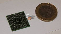
At the ongoing IFA event in Berlin, AMD displayed one of the first derivatives of its Bobcat low-power x86 processor architecture, codenamed "Ontario". This Fusion APU (accelerated processing unit), which is a combination of an x86 CPU and a DirectX 11 compliant GPU is built for low-power devices such as netbooks, handhelds, and tablets. AMD also showed off the chip package itself, which is roughly the size of a 1 Euro coin. The package, like AMD's mobile Athlon/Phenom processors, has no integrated heatspreader (IHS), but like the Intel Atom, uses a ball-grid array (BGA) to permanently fix itself to the system board.
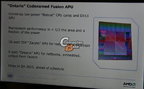
AMD claims that the chip offers "mainstream performance" at less than half the die area (in this case, below 100 mm²), and a fraction of the power. Speaking of which, the "Ontario" Fusion APU has a TDP of 9W, while a higher-performance APU codenamed "Zacate", which is probably competitive with Intel's CULV processors, and is built for ultra-thin notebooks, nettops and slim all-in-one PCs, has a TDP of 18W. AMD claims that the two will ship (to OEMs, because these are not end-user products) in Q4 2010. For the desktop, AMD is developing the "Llano" Fusion APUs that are of a different form-factor and package altogether.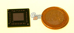
AMD claims that the chip offers "mainstream performance" at less than half the die area (in this case, below 100 mm²), and a fraction of the power. Speaking of which, the "Ontario" Fusion APU has a TDP of 9W, while a higher-performance APU codenamed "Zacate", which is probably competitive with Intel's CULV processors, and is built for ultra-thin notebooks, nettops and slim all-in-one PCs, has a TDP of 18W. AMD claims that the two will ship (to OEMs, because these are not end-user products) in Q4 2010. For the desktop, AMD is developing the "Llano" Fusion APUs that are of a different form-factor and package altogether.