News Posts matching #Bulldozer

Return to Keyword Browsing

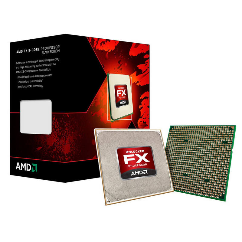
AMD FX-8350 Pushed to 8.1 GHz via Extreme Overclocking by Der8auer

AMD's Bulldozer architecture is a well-known quantity by now, and seemingly straddles a line between loathing and love between tech enthusiasts. Slow and power hungry compared to Intel's options, it harkens back to a time where the roles were reversed, and AMD were looking to compensate for architectural deficiencies (and architectural design decisions that can either be claimed as erroneous or ahead of their time) via increased clockspeeds. However you look at these Bulldozer CPUs, the fact is that they remain some of the best overclockers of all time - at least when it comes to maximum operating frequencies, especially at absolutely scorching vCore values.

To achieve that operating frequency, Der8auer used an Elmor EVC2 controller and diagnostics chip, which, connected to a usually unpopulated pin area in the ASUS 970 PRO GAMING/AURA motherboard, allowed him to read-out everything that was running through the motherboard's VRM circuitry, and perform manual adjustments. Corsair Vengeance 2,666 MHz DDR3 memory was also used in the system. An accident happened along the way, though: when pulling AMD's stock cooler from the motherboard, the CPU remained attached to the cooler, which resulted in some bent pins (screams in horror). Luckily, things were fixed with a screwdriver - let that serve as a warning, alert, and tip, should this happen to you.

AMD Processors Since 2011 Hit with Cache Attack Vulnerabilities: Take A Way

Cybersecurity researcher Moritz Lipp and his colleagues from the Graz University of Technology and the University of Rennes uncovered two new security vulnerabilities affecting all AMD CPU microarchitectures going back to 2011, detailed in a research paper titled "Take A Way." These include "Bulldozer" and its derivatives ("Piledriver," "Excavator," etc.,) and the newer "Zen," "Zen+," and "Zen 2" microarchitectures. The vulnerabilities are specific to AMD's proprietary L1D cache way predictor component. It is described in the security paper's abstract as a means for the processor to "predict in which cache way a certain address is located, so that consequently only that way is accessed, reducing the processor's power consumption."

By reverse engineering the L1D cache way predictor in AMD microarchitectures dating from 2011 to 2019, Lipp, et al, discovered two new attack vectors with which an attacker can monitor the victim's memory accesses. These vectors are named "Collide+Probe," and "Load+Reload." The paper describes the first vector as follows: "With Collide+Probe, an attacker can monitor a victim's memory accesses without knowledge of physical addresses or shared memory when time-sharing a logical core." The second vector is described as "With Load+Reload, we exploit the way predictor to obtain highly-accurate memory-access traces of victims on the same physical core." The two vulnerabilities have not been assigned CVE entries at the time of this writing. The research paper, however, describes the L1D cache way predictor in AMD processors as being vulnerable to attacks that can reveal contents of memory or even keys to a vulnerable AES implementation. For now there is no mitigation to these attacks, but the company is reportedly working on firmware and driver updates. Access the research paper here.
AMD L1D cache way predictor logic found vulnerable in Take A Way attack classes.

AMD to Cough Up $12.1 Million to Settle "Bulldozer" Core Count Class-Action Lawsuit

AMD reached a settlement in the Class Action Lawsuit filed against it, over alleged false-marketing of the core-counts of its eight-core FX-series processors based on the "Bulldozer" microarchitecture. Each member of the Class receives a one-time payout of USD $35 per chip, while the company takes a hit of $12.1 million. The lawsuit dates back to 2015, when Tony Dickey, representing himself in the U.S. District Court for the Northern District of California, accused AMD of false-marketing of its FX-series "Bulldozer" processor of having 8 CPU cores. Over the following four years, the case gained traction as a Class Action was built against AMD this January.

In the months that followed the January set-up of a 12-member Jury to examine the case, lawyers representing the Class and AMD argued over the underlying technology that makes "Bulldozer" a multi-core processor, and eventually discussed what a fair settlement would be for the Class. They eventually agreed on a number - $12.1 million, or roughly $35 per chip AMD sold, which they agreed was "fair," and yet significantly less than the "$60 million in premiums" consumers contended they paid for these processors. Sifting through these numbers, it's important to understand what the Class consists of. It consists of U.S. consumers who became interested to be part of the Class Action, and who bought an 8-core processor based on the "Bulldozer" microarchitecture. It excludes consumers of every other "Bulldozer" derivative (4-core, 6-core parts, APUs; and follow-ups to "Bulldozer" such as "Piledriver," "Excavator," etc.).
Image Credit: Taylor Alger

MSI CEO: AMD Plans to Stop Being the Value Alternative, X570 Motherboards to be Expensive

MSI's CEO Charles Chiang, quoted by Tom's Hardware at COMPUTEX 2019, laid out what we were already seeing with motherboard designs from all vendors of AMD's X570-based motherboards: pricing is likely increasing across the board, and AMD's market positioning won't be of the alternative, lower-value brand.

As quoted, Chiang said that ""Lots of people ask me, what do you think about today's AMD? I say today's AMD is completely different company compared to two, three, five years ago. They have nice technology and they are there to put the higher spec with the reasonable pricing. But right now they say, "Hey Charles, let's push to marketing to the higher [end]. So let's sell higher-pricing motherboards, higher-spec motherboards, and let's see what will happen in the market. So I don't think that AMD is the company that wants to sell low cost here, low cost there." Which does make sense: AMD isn't in the position of the underdog anymore -at least technology and product-portfolio wise when it comes to consumer CPUs. With better products, comes a desire for higher margins, and a change in direction for a company that was basically forced to almost cut itself out of the market in terms of profits with its previous, non-competitive CPU designs.

Bulldozer Core-Count Debate Comes Back to Haunt AMD

AMD in 2012 launched the FX-8150, the "world's first 8-core desktop processor," or so it says on the literal tin. AMD achieved its core-count of 8 with an unconventional CPU core design. Its 8 cores are arranged in four sets of two cores each, called "modules." Each core has its own independent integer unit and L1 data cache, while the two cores share a majority of their components - the core's front-end, a branch-predictor, a 64 KB L1 code cache, a 2 MB L2 cache, but most importantly, an FPU. There was much debate across tech forums on what constitutes a CPU core.

Multiprocessor-aware operating systems had to be tweaked on how to properly address a "Bulldozer" processor. Their schedulers would initially treat "Bulldozer" cores as fully independent (as conventional logic would dictate), until AMD noticed multi-threaded application performance bottlenecks. Eventually, Windows and various *nix kernels received updates to their schedulers to treat each module as a core, and each core as an SMT unit (a logical processor). The FX-8350 is a 4-core/8-thread processor in the eyes of Windows 10, for example. These updates improved the processors' performance but not before consumers started noticing that their operating systems weren't reporting the correct core-count. In 2015, a class-action lawsuit was filed against AMD for false marketing of FX-series processors. The wheels of that lawsuit are finally moving, after a 12-member Jury is set up to examine what constitutes a CPU core, and whether an AMD FX-8000 or FX-9000 series processor can qualify as an 8-core chip.

Intel Unveils a Clean-slate CPU Core Architecture Codenamed "Sunny Cove"

Intel today unveiled its first clean-slate CPU core micro-architecture since "Nehalem," codenamed "Sunny Cove." Over the past decade, the 9-odd generations of Core processors were based on incrementally refined descendants of "Nehalem," running all the way down to "Coffee Lake." Intel now wants a clean-slate core design, much like AMD "Zen" is a clean-slate compared to "Stars" or to a large extent even "Bulldozer." This allows Intel to introduce significant gains in IPC (single-thread performance) over the current generation. Intel's IPC growth curve over the past three micro-architectures has remained flat, and only grew single-digit percentages over the generations prior.

It's important to note here, that "Sunny Cove" is the codename for the core design. Intel's earlier codenaming was all-encompassing, covering not just cores, but also uncore, and entire dies. It's up to Intel's future chip-designers to design dies with many of these cores, a future-generation iGPU such as Gen11, and a next-generation uncore that probably integrates PCIe gen 4.0 and DDR5 memory. Intel details "Sunny Cove" as far as mentioning IPC gains, a new ISA (new instruction sets and hardware capabilities, including AVX-512), and improved scalability (ability to increase core-counts without running into latency problems).

Intel to Accelerate Basin Falls Unveil, Coffee Lake Launch

According to DigiTimes, sources among Taiwan-based PC vendors have indicated that Intel's upcoming Basin Falls platform, which includes Skylake-X and Kaby Lake-X processors on a new X299 chipset, will be unveiled at Computex 2017 (May 30th, June 3rd), in Taipei - two months earlier than expected. This move comes accompanied by an accelerated launch of the Coffee Lake microarchitecture, which still uses the 14 nm process, to August 2017 from an initial January 2018 launch. If true, this is big in a number of ways - that Intel would bring forward a product launch 4 months has some interesting implications - or at least, confirmations.

Remember that Coffee Lake is supposed to carry an increased number of cores in its mainstream designs. And we all know how Intel's line-up has almost been torn apart by Ryzen's aggressive core and thread-count, with AMD offering more cores and threads than Intel at virtually all price-points. And even if an argument is made regarding Intel's better gaming performance, that's one scenario out of many. Future proofing, professional work, multimedia, all of these assert AMD's dominance in a pure price-performance ratio. I, for one, would gladly give up some FPS in some games and accept an increased number of cores than go the other way around (especially with AMD's platform support and the number of patches that have increased game performance on Ryzen CPUs.)

AMD Ryzen Machine Crashes to a Sequence of FMA3 Instructions

An AMD Ryzen 7-1800X powered machine was found to be crashing upon execution of a very specific set of FMA3 instructions by Flops version 2, a simple open-source CPU benchmark by Alexander "Mystical" Yee. An important point to note here is that this little known benchmark has been tailored by its developer to be highly specific to the CPU micro-architecture, with separate binaries for each major x64 architecture (eg: Bulldozer, Sandy Bridge, Haswell, Skylake, etc.), and as such the GitHub repository does not have a "Zen" specific binary.

Members of the HWBot forums found that Ryzen powered machines crash on running the Haswell-specific binary, at "Single-Precision - 128-bit FMA3 - Fused Multiply Add." The Haswell-specific binary (along with, we imagine, Skylake), adds support for the FMA3 instruction-set, which Ryzen supports, and which lends some importance to the discovery of this bug. What also makes this important is because a simple application, running at user privileges (i.e. lacking special super-user/admin privileges), has the ability to crash the machine. Such a code could even be executed through virtual machines, and poses a security issue, with implications for AMD's upcoming "Naples" enterprise processor launch.

AMD Talks Zen 3, "Raven Ridge," and More at Reddit AMA

AMD, at its post-Ryzen 7 launch Reddit AMA, disclosed some juicy details about its other upcoming socket AM4 chips, beginning with the rest of the Ryzen 5 and Ryzen 3 "Summit Ridge" processor roll-out, and a little bit about its 8th generation socket AM4 APU, codenamed "Raven Ridge." To begin with, AMD CEO Lisa Su stated that "Raven Ridge" will also be sold under the Ryzen brand. This would mark a departure from the less-than-stellar A-series branding for its performance APUs. "Raven Ridge" likely combines a "Zen" quad-core CPU complex (CCX) with an integrated GPU based on one of AMD's newer GPU architectures (either "Polaris" or "Vega").

The range-topping Ryzen 7 series will lead the company's lineup throughout Q1, with six-core and quad-core Ryzen 5 and Ryzen 3 series launches being scheduled for later this year. Our older reports pinned Ryzen 5 series rollout for Q2, and Ryzen 3 series for the second half of 2017. This is likely also when the company rolls out "Raven Ridge" initially as mobile Ryzen products (BGA packages, which will likely also be used in AIOs), and later as desktop socket AM4 parts.

AMD's Upcoming Ryzen Line-up Could Feature 6-Core Chips After All

It's always a dance between rumours, expectations and "theorycrafting" when it comes to the launch of any particularly exciting product. And with AMD's Ryzen chips currently being the most hotly anticipated development (and product launch) in the hardware world, well, let's just say that anticipation is really building up to enormous levels, with any possible details surrounding AMD's line-up being the cause, in some cases, of heated debate.

Case in point: with AMD's CCX (CPU Complex) being indivisible, this would mean a blow not only to budget-conscious consumers, but also to AMD's ability to engender its product line. Flexibility has always been the name of the game with AMD (discounting their CMT-based Bulldozer and derived architectures), with the company offering triple-core processors in the past (and weren't those the good old days of processor unlocking). However, now reports have come in that Ryzen's CCX are actually divisible, which could open up possibilities for some theoretically value-breaking hexa-core Ryzen chips.

AMD Says "ZEN" CPU Architecture is Expected to Last 4 Years

After spending almost 4 years developing and perfecting (as much as can be perfected in such an amount of time) it's ZEN CPU architecture, AMD is looking to extract some mileage out of it. Mark Papermaster, AMD's chief technology officer, confirmed the four-year lifespan in a conversation with PC World at CES 2017 in Las Vegas, though he declined to discuss specifics. When asked how long ZEN would last (especially comparing to Intel's now-failing two-year tick-tock cadence, Papermaster confirmed the four-year lifespan: "We're not going tick-tock," he said. "ZEN is going to be tock, tock, tock."

AMD Details ZEN Microarchitecture IPC Gains

AMD Tuesday hosted a ZEN microarchitecture deep-dive presentation in the backdrop of Hot Chips, outlining its road to a massive 40 percent gain in IPC (translated roughly as per-core performance gains), over the current "Excavator" microarchitecture. The company credits the gains to three major changes with ZEN: better core engine, better cache system, and lower power. With ZEN, AMD pulled back from its "Bulldozer" approach to cores, in which two cores share certain number-crunching components to form "modules," and back to a self-sufficient core design.

Beyond cores, the next-level subunit of the ZEN architecture is the CPU-Complex (CCX), in which four cores share an 8 MB L3 cache. This isn't different from current Intel architectures, the cores share nothing beyond L3 cache, making them truly independent. What makes ZEN a better core, besides its independence from other cores, and additional integer pipelines; subtle upscaling in key ancillaries such as micro-Op dispatch, instruction schedulers; retire, load, and store queues; and a larger quad-issue FPU.

AMD ZEN Quad-Core Subunit Named CPU-Complex (CCX)

We've been chasing AMD Zen for a long time now. Our older report from April 2015 uncovered an important detail about component organization on Zen processors - the clumping of four CPU cores into a highly-specialized, possibly indivisible subunit referred to then, as the "Zen Quad-core Unit." Some of the latest presentations about the architecture, following AMD's "performance reveal" event from earlier this month, shed more light on this quad-core unit.

AMD is referring to the Zen quad-core unit as the CPU-Complex (CCX). Each CCX is a combination of four independent CPU cores. Unlike on "Bulldozer," a "Zen" core does not share any of its number-crunching machinery with neighboring cores. Each "Zen" core has a dedicated L2 cache of 512 KB, and four Zen cores share an 8 MB L3 cache. AMD will control core-counts by controlling CCX units. A "Summit Ridge" socket AM4 processor features two CCX units (making up eight cores in all), sharing a dual-channel DDR4 memory controller, and the platform core-logic (chipset), complete with an integrated PCI-Express root complex. Socket AM4 APUs will feature one CCX unit, and an integrated GPU in place of the second CCX. With this, AMD is able to bring the two diverse desktop platforms under one socket.

AMD Dragged to Court over Core Count on "Bulldozer"

This had to happen eventually. AMD has been dragged to court over misrepresentation of its CPU core count in its "Bulldozer" architecture. Tony Dickey, representing himself in the U.S. District Court for the Northern District of California, accused AMD of falsely advertising the core count in its latest CPUs, and contended that because of they way they're physically structured, AMD's 8-core "Bulldozer" chips really only have four cores.

The lawsuit alleges that Bulldozer processors were designed by stripping away components from two cores and combining what was left to make a single "module." In doing so, however, the cores no longer work independently. Due to this, AMD Bulldozer cannot perform eight instructions simultaneously and independently as claimed, or the way a true 8-core CPU would. Dickey is suing for damages, including statutory and punitive damages, litigation expenses, pre- and post-judgment interest, as well as other injunctive and declaratory relief as is deemed reasonable.

AMD "Zen" CPU Prototypes Tested, "Meet all Expectations"

AMD reportedly finished testing some of its first "Zen" micro-architecture CPU prototypes, and concluded that they "meet all expectations," with "no significant bottlenecks found" in its design. This should mean that AMD's "Zen" chips should be as competitive with Intel chips as it set them out to be. The company is planning to launch its first client CPUs based on the "Zen" micro-architecture in 2016, based on its swanky new AM4 socket, with DDR4 memory and integrated PCIe (a la APUs). Zen sees AMD revert to the large, monolithic core design, from its "Bulldozer" multi-core module design with a near doubling of number-crunching machinery per-core, compared to its preceding architecture.

AMD Zen Features Double the Per-core Number Crunching Machinery to Predecessor

AMD "Zen" CPU micro-architecture has a design focus on significantly increasing per-core performance, particularly per-core number-crunching performance, according to a 3DCenter.org report. It sees a near doubling of the number of decoder, ALU, and floating-point units per-core, compared to its predecessor. In essence, the a Zen core is AMD's idea of "what if a Steamroller module of two cores was just one big core, and supported SMT instead."

In the micro-architectures following "Bulldozer," which debuted with the company's first FX-series socket AM3+ processors, and running up to "Excavator," which will debut with the company's "Carrizo" APUs, AMD's approach to CPU cores involved modules, which packed two physical cores, with a combination of dedicated and shared resources between them. It was intended to take Intel's Core 2 idea of combining two cores into an indivisible unit further.

AMD to Emphasize on "Generation" with Future CPU Branding

AMD is planning to play a neat branding game with Intel. Branding of the company's 2016 lineup of CPUs and APUs will emphasize on "generation," much in the same way Intel does with its Core processor family. AMD will mention in its PIB product packaging, OEM specs sheets, and even its product logo (down to the case-badge), that its 2016 products (FX-series CPUs and A-series APUs) are the company's "6th generation." 2016 marks prevalence of Intel's Core "Skylake" processor family, which is its 6th generation Core family (succeeding Nehalem/Westmere, Sandy Bridge, Ivy Bridge, Haswell, and Broadwell). AMD is arriving at its "6th generation" moniker counting "Stars," "Bulldozer," "Piledriver," "Steamroller," and "Excavator," driving its past 5 generations of APUs, and the occasional FX CPU.

It turns out that the emphasis on "generation" is big with DIY and SI retail channels. Retailers we spoke with, say that they find it easier to break through Intel's often-confusing CPU socket change cycle, which ticks roughly every 18-24 months. Customers, they say, find it easier to simply mention the "generation" of Core processor they want, to get all relevant components to go with them (such as motherboard and memory bundles). While AMD's FX brand clearly didn't see generations beyond "Piledriver," the company's decision to unify the socket for its FX and A-Series product lines next year, with AM4, makes "6th generation FX processor" valid.

First AMD "Zen" Chips to be Quad-Core

Some of the first CPUs and APUs based on AMD's next-generation "Zen" micro-architecture could be quad-core. "Zen" will be AMD's first monolithic core design after a stint with multi-core modules, with its "Bulldozer" architecture. Our older article details what sets Zen apart from its predecessor. As expected, in a multi-core chip, Zen cores share no hardware resources with each other, than a last-level cache (L3 cache), much like Intel's current CPU architecture.

There's just one area where Zen will differ from Haswell. With Haswell, Intel has shown that it can clump any number of cores on a chip, and make them share a proportionately large L3 cache. Haswell-E features 8 cores sharing a 20 MB cache. The Haswell-EX features 18 cores sharing 45 MB of cache. With Zen, however, the scale up stops at 4 cores sharing 8 MB of L3 cache. A set of four cores makes up what AMD calls a "quad-core unit." To be absolutely clear, this is not a module, the cores share no hardware components with each other, besides the L3 cache.

AMD "Zen" CPU Core Block Diagram Surfaces

As a quick follow up to our older report on AMD's upcoming "Zen" CPU core micro-architecture being a reversion to the monolithic core design, and a departure from its "Bulldozer" multicore module design which isn't exactly flying off the shelves, a leaked company slide provides us the first glimpse into the core design. Zen looks a lot like "Stars," the core design AMD launched with its Phenom series, except it has a lot more muscle, and one could see significant IPC improvements over the current architecture.

To begin with, Zen features monolithic fetch and decode units. On Bulldozer, two cores inside a module featured dedicated decode and integer units with shared floating-point units. On Zen, there's a monolithic decode unit, and single integer and floating points. The integer unit has 6 pipelines, compared to 4 per core on Bulldozer. The floating point unit has two large 256-bit FMAC (fused-multiply accumulate) units, compared to two 128-bit ones on Bulldozer. The core has a dedicated 512 KB L2 cache. This may be much smaller than the 2 MB per module on Bulldozer, but also indicate that the core is able to push through things fast enough to not need cushioning by a cache (much like Intel's Haswell architecture featuring just 256 KB per core). In a typical multi-core Zen chip, the cores will converge at a large last-level cache, which routes data between them to the processor's uncore, which will feature a DDR4 IMC and a PCI-Express 3.0 root complex.

AMD "Zen" A Monolithic Core Design

AMD's upcoming "Zen" architecture will see a major change in the way the company designs its CPU cores. It will be a departure from the "module" core design introduced with "Bulldozer," in which two cores with shared resources constitute the indivisible unit of a multi-core processor. A "Zen" core will have dedicated resources in a way things used to be before "Bulldozer," and only the last-level cache (L3 cache), will be shared between cores. "Zen" will also implement SMT, much in the same way as Intel processors do, with HyperThreading Technology.

The first implementation of "Zen" will be an insanely powerful APU (on paper anyway), featuring 16 physical "Zen" CPU cores, 32 logical CPUs enabled with SMT, 512 KB dedicated L2 cache per core, and 32 MB of shared L3 cache. The CPU's ISA instruction set will see a spring-cleaning, with the removal of underused instruction-sets, and the introduction of new ones. Other features on this APU are equally surprising - a quad-channel DDR4 integrated memory controller, a separate HBM (high-bandwidth memory) controller dedicated to the integrated graphics, with up to 512 GB/s bandwidth, and an integrated graphics core featuring "Greenland-class" stream processors. Given that AMD is able to build 7-billion transistor GPUs on existing 28 nm processes, building an APU with these chops doesn't sound far-fetched. The company could still have to rely on a newer fab.

AMD to Switch to GlobalFoundries' 28 nm SHP Node in 2015

Faced with continuous development roadblocks with TSMC, AMD is reportedly planning to switch to the 28 nm SHP process of GlobalFoundries, to build GPUs in 2015. The 28 nm SHP (super high-performance) node will allow the company to lower voltages, giving it greater room to increase clock speeds of its upcoming GPUs. AMD's GPUs in 2015 could be based on its latest Graphics CoreNext 1.2 architecture, and AMD needs every means to minimize voltages, and crank up clock speeds.

The company hasn't abandoned TSMC completely just yet, with reports speaking of AMD using the Taiwanese fab's 16 nm FinFet node to manufacture its next-generation "Zen" CPUs. Zen is the successor to AMD's "Bulldozer" architecture and its derivatives ("Piledriver" and "Steamroller.") It could feature a radically different core design.

SHARKOON Releases the Bulldozer Midi-Tower PC Case

SHARKOON Technologies has now made available the Bulldozer, a midi-tower PC chassis for gamers and enthusiasts that are on a tighter budget. This new case measures 480 (L) x 235 (W) x 460 (H) mm, it weighs 6.5 kg and features a front I/O panel with two USB 3.0 and two USB 2.0 ports, two 5.25-inch drive bays, and seven (4 x 2.5-inch and 3 x 3.5-inch) internal drive trays.

SHARKOON's case also has an acrylic side window, two (red, blue or green-colored) 120 mm fans (front and back), and it offers support for graphics cards up to 415 mm long. The Bulldozer comes in three color schemes (black/red, black/blue, black/green) and costs 49.99 Euro.

Engineering Sample Of AMD Steamroller Based APU Spotted

Hardware news site WCCF Tech spotted an interesting entry listed in the Bionic research database. The ES (Engineering Sample) chip could be a part of AMD's next-generation APU series featuring the new and improved Steamroller core. While we don't expect performance to increase by leaps and bounds, but Steamroller builds on the Bulldozer architecture and has a target to offer as much as a 30% improvement in performance over the original core.
The ES code 2M186092H4467_23/18/12/05_1304 tells us even more. According to earlier observations (here and here), the four numbers in the middle part tell a bit about clock speeds. If the first one is not 00 (no turbo, see Kabini ES), it indicates a turbo clock of 2.3GHz. The "18? stands for 1.8GHz nominal frequency. I'm not so sure about the "12?. It could stand for 1.2Ghz North Bridge clock. Finally the "05? indicates a 500MHz GPU clock. The right part "1304? is the GPU code, which - thanks to earlier revelations - can be identified as AMD1304.1 = "KV SPECTRE MOBILE 35W (1304)".
A 2.3 GHz Turbo core is pretty low, which can be attributed to the early state of the Engineering Sample. Hopefully clock speeds hit further north of just 1.8 GHz CPU and 500 MHz graphics, especially for the 35W part. The next-generation chips will be manufactured on the new bulk 28nm manufacturing process at Global Foundries.

AMD Super Pi History To Be Rewritten, Courtesy The Stilt

AMD Super Pi History To Be Rewritten, Courtesy Of The Stilt

AMD's typically underwhelming Super PI performance, that was usually attributed to architectural limitations when it comes to the X87 instruction set, appears to have been nothing more than a blunder on the part of the developers responsible with BIOS development and optimization for AMD platforms. Finnish overclocker, The Stilt, figured out how to considerably improve performance by going through the BIOS developers guides. The exact same guides available to the BIOS R&D teams of motherboard vendors, a surprising fact considering a single man managed to outdo an entire industry. Here is the download link to the patch: click

The Stilt posted a video in which he showed a 4.1GHz A10-6800K completing SuperPI in 17 minutes and 34 seconds. The fastest 5GHz Richland SuperPI 32M is around 18 minutes and 15 seconds. A lot faster! For more information, check out the thread in the HWBot forums.

APUs Make Up Nearly 75% of AMD's Processor Sales

Despite losing in market share to Intel, AMD has reason to cheer as its APU gambit is beginning to pay off. According to the latest architecture- and core count-specific sales figures for AMD given out by Mercury Research detailing Q3-2013 in context of two preceding quarters, APUs make for nearly 75% of AMD's processor sales, and the company's recently-launched "Trinity" line of desktop and mobile APUs are off to a flying start.

The most popular chips in AMD's stable are its "Bobcat" Zacate series low-power APUs, which are being built into entry-level computing devices such as netbooks, nettops, and all-in-one desktops. The chips make up 39 percent of AMD's sales in Q3, followed by another APU line, the A-Series "Trinity", which is available in desktop and mobile variants, offers a combination of a fast integrated graphics processor with up to four CPU cores, and makes up 26.1 percent of AMD's sales. AMD's A-Series "Llano" can still be bought in the market, and makes up 7.4 percent of AMD's sales in Q3.
Return to Keyword Browsing
May 2nd, 2024 01:07 EDT change timezone

New Forum Posts

Popular Reviews

Controversial News Posts