News Posts matching #CXL

Return to Keyword Browsing

Intel "Sapphire Rapids" Xeon Processor Could Feature Up To 80 Cores: New Leak

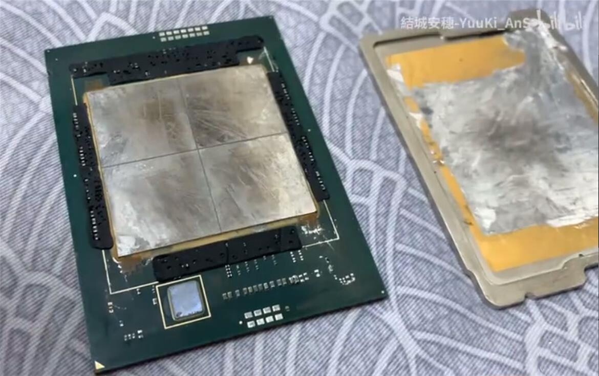
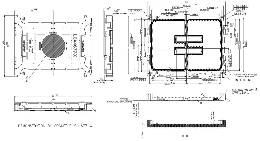
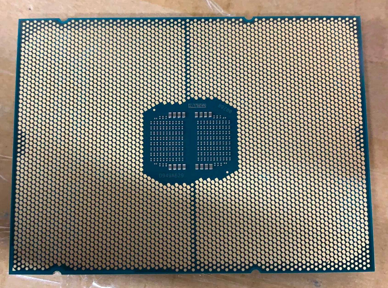
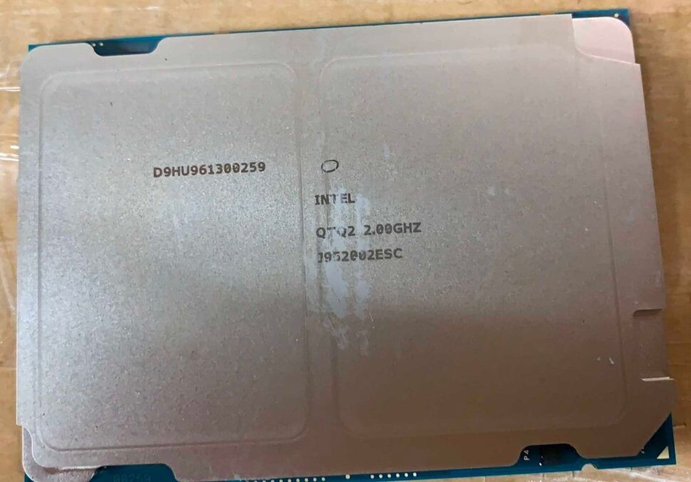
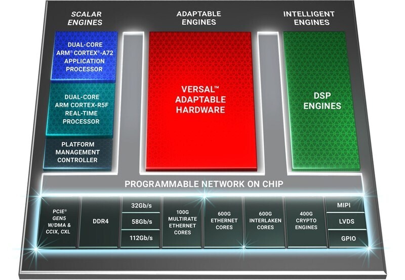
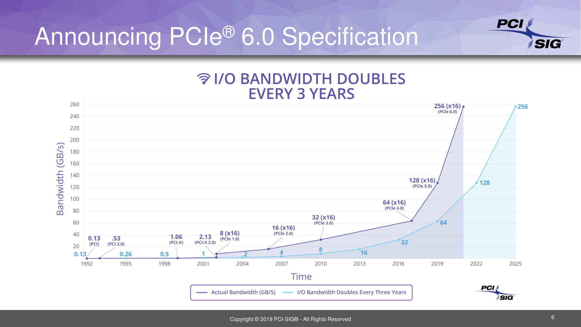
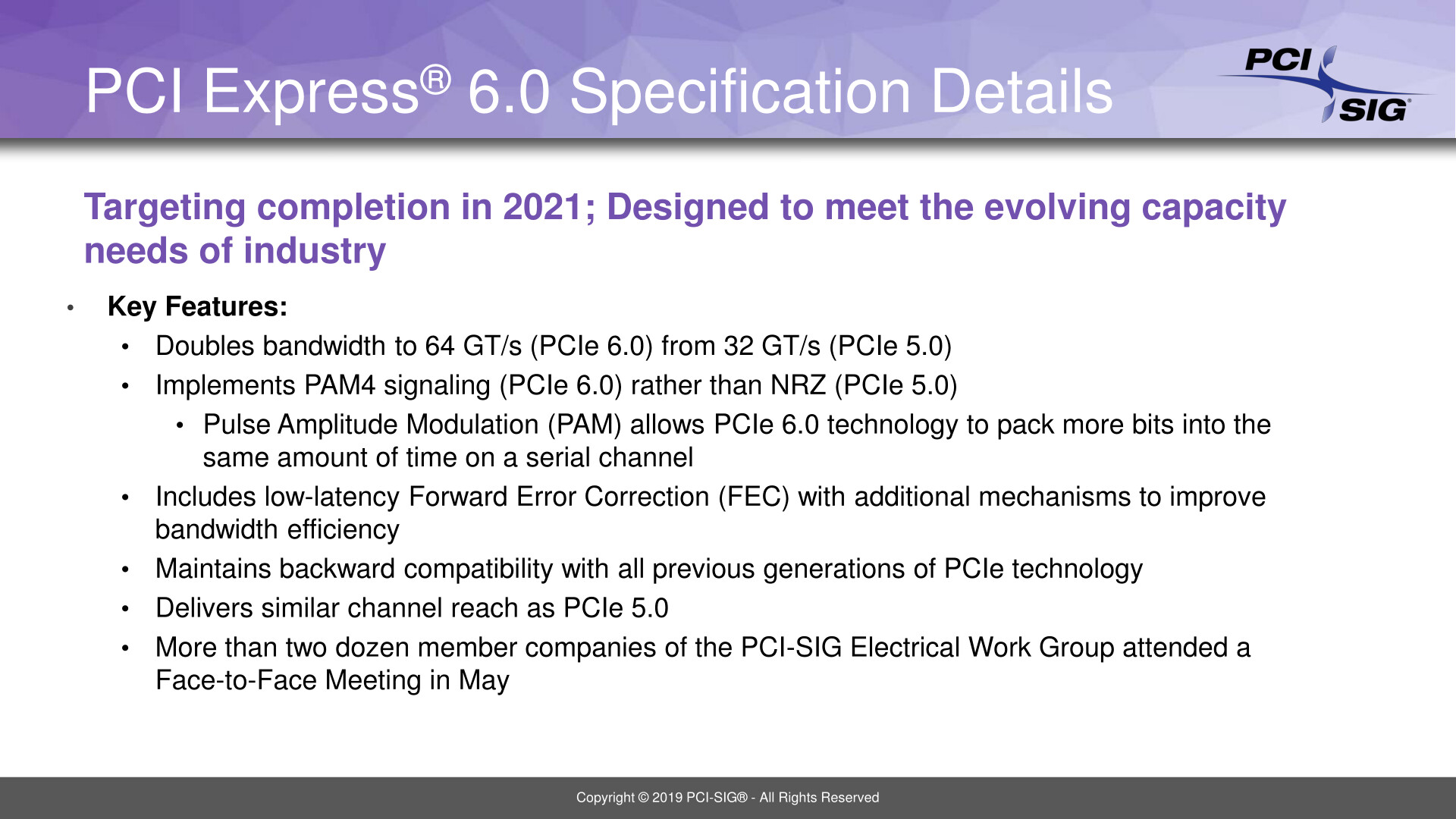
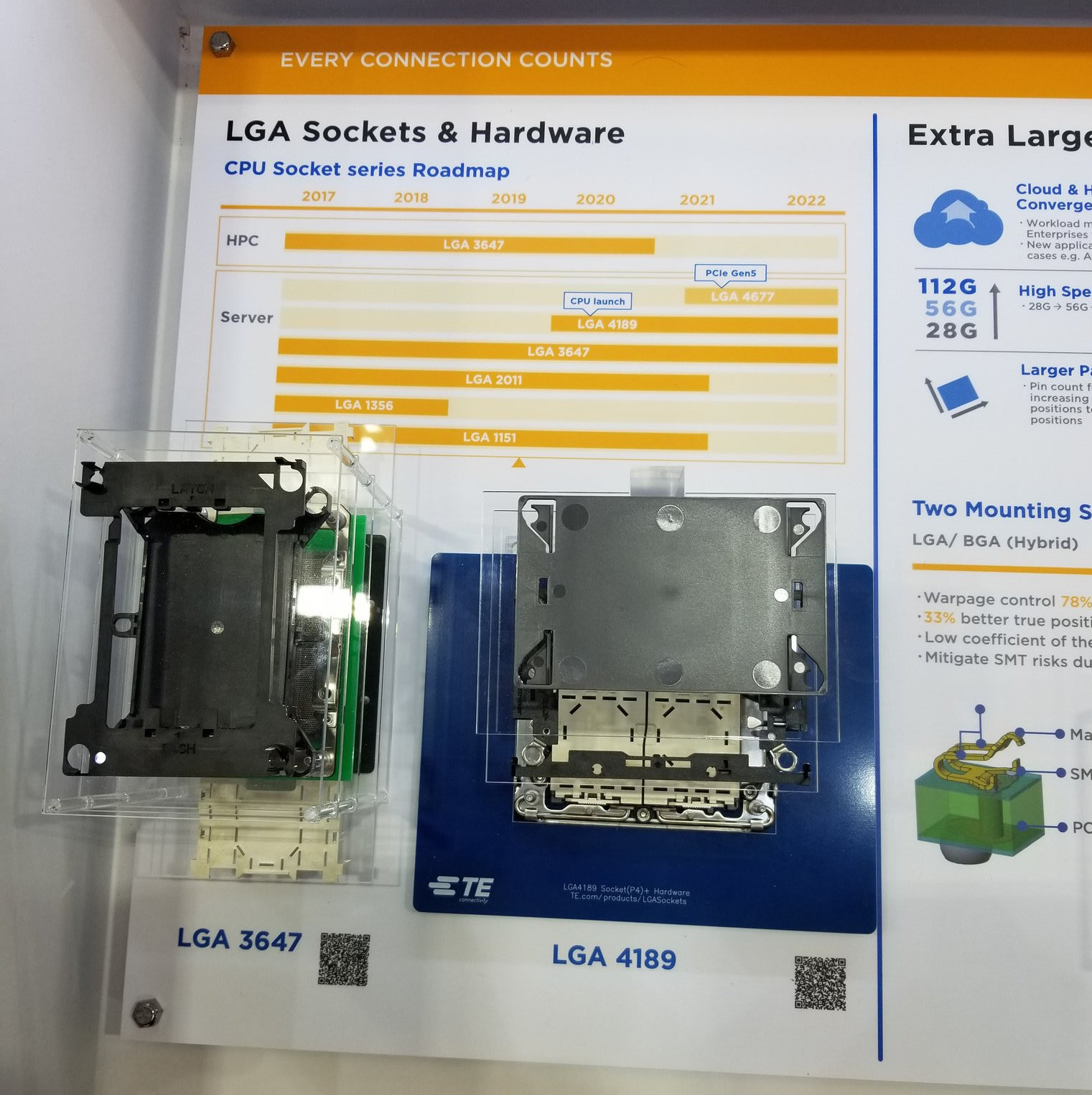
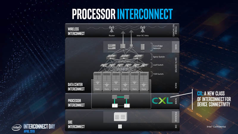
Intel's upcoming Xeon "Sapphire Rapids" enterprise processor come come with CPU core-counts as high as 80, according to the latest round of photo-leaks. An earlier article predicted the chip cram up to 56 cores alongside on-package HBM. The processor reportedly features up to 80 cores, spread across four 20-core chiplets. Unlike on the latest AMD EPYC processor, there doesn't appear to be a centralized I/O controller die. This particular processor is based in the LGA4189 package, which features additional pins compared to the LGA4577-X socket from the 56-core leak. The newer socket has additional pins that enable next-gen I/O, which include PCI-Express Gen 5.0, and CXL 1.1 interface.

Microchip Announces World's First PCI Express 5.0 Switches

Applications such as data analytics, autonomous-driving and medical diagnostics are driving extraordinary demands for machine learning and hyperscale compute infrastructure. To meet these demands, Microchip Technology Inc. today announced the world's first PCI Express (PCIe) 5.0 switch solutions—the Switchtec PFX PCIe 5.0 family—doubling the interconnect performance for dense compute, high speed networking and NVM Express (NVMe ) storage. Together with the XpressConnect retimers, Microchip is the industry's only supplier of both PCIe Gen 5 switches and PCIe Gen 5 retimer products, delivering a complete portfolio of PCIe Gen 5 infrastructure solutions with proven interoperability.

"Accelerators, graphic processing units (GPUs), central processing units (CPUs) and high-speed network adapters continue to drive the need for higher performance PCIe infrastructure. Microchip's introduction of the world's first PCIe 5.0 switch doubles the PCIe Gen 4 interconnect link rates to 32 GT/s to support the most demanding next-generation machine learning platforms," said Andrew Dieckmann, associate vice president of marketing and applications engineering for Microchip's data center solutions business unit. "Coupled with our XpressConnect family of PCIe 5.0 and Compute Express Link (CXL ) 1.1/2.0 retimers, Microchip offers the industry's broadest portfolio of PCIe Gen 5 infrastructure solutions with the lowest latency and end-to-end interoperability."

Intel Xeon "Sapphire Rapids" LGA4677-X Processor Sample Pictured

Here are some of the first pictures of the humongous Intel Xeon "Sapphire Rapids-SP" processor, in the flesh. Pictured by YuuKi-AnS on Chinese micro-blogging site bilibili, the engineering sample looks visibly larger than an AMD EPYC. Bound for 2021, this processor will leverage the latest generation of Intel's 10 nm Enhanced SuperFin silicon fabrication node, the latest I/O that include 8-channel DDR5 memory, a large number of PCI-Express gen 5.0 lanes, and ComputeXpress Link (CXL) interconnect. Perhaps the most interesting bit of information from the YuuKi-AnS has to be the mention of an on-package high-bandwidth memory solution. The processors will introduce an IPC uplift over "Ice Lake-SP" processors, as they use the newer "Willow Cove" CPU cores.

Intel Confirms HBM is Supported on Sapphire Rapids Xeons

Intel has just released its "Architecture Instruction Set Extensions and Future Features Programming Reference" manual, which serves the purpose of providing the developers' information about Intel's upcoming hardware additions which developers can utilize later on. Today, thanks to the @InstLatX64 on Twitter we have information that Intel is bringing on-package High Bandwidth Memory (HBM) solution to its next-generation Sapphire Rapids Xeon processors. Specifically, there are two instructions mentioned: 0220H - HBM command/address parity error and 0221H - HBM data parity error. Both instructions are there to address data errors in HBM so the CPU operates with correct data.

The addition of HBM is just one of the many new technologies Sapphire Rapids brings. The platform is supposedly going to bring many new technologies like an eight-channel DDR5 memory controller enriched with Intel's Data Streaming Accelerator (DSA). To connect to all of the external accelerators, the platform uses PCIe 5.0 protocol paired with CXL 1.1 standard to enable cache coherency in the system. And as a reminder, this would not be the first time we see a server CPU use HBM. Fujitsu has developed an A64FX processor with 48 cores and HBM memory, and it is powering today's most powerful supercomputer - Fugaku. That is showing how much can a processor get improved by adding a faster memory on-board. We are waiting to see how Intel manages to play it out and what we end up seeing on the market when Sapphire Rapids is delivered.

Alleged Intel Sapphire Rapids Xeon Processor Image Leaks, Dual-Die Madness Showcased

Today, thanks to the ServeTheHome forum member "111alan", we have the first pictures of the alleged Intel Sapphire Rapids Xeon processor. Pictured is what appears to be a dual-die design similar to Cascade Lake-SP design with 56 cores and 112 threads that uses two dies. The Sapphire Rapids is a 10 nm SuperFin design that allegedly comes even in the dual-die configuration. To host this processor, the motherboard needs an LGA4677 socket with 4677 pins present. The new LGA socket, along with the new 10 nm Sapphire Rapids Xeon processors are set for delivery in 2021 when Intel is expected to launch its new processors and their respective platforms.

The processor pictured is clearly a dual-die design, meaning that Intel used some of its Multi-Chip Package (MCM) technology that uses EMIB to interconnect the silicon using an active interposer. As a reminder, the new 10 nm Sapphire Rapids platform is supposed to bring many new features like a DDR5 memory controller paired with Intel's Data Streaming Accelerator (DSA); a brand new PCIe 5.0 standard protocol with a 32 GT/s data transfer rate, and a CXL 1.1 support for next-generation accelerators. The exact configuration of this processor is unknown, however, it is an engineering sample with a clock frequency of a modest 2.0 GHz.

CXL Consortium Releases Compute Express Link 2.0 Specification

The CXL Consortium, an industry standards body dedicated to advancing Compute Express Link (CXL) technology, today announced the release of the CXL 2.0 specification. CXL is an open industry-standard interconnect offering coherency and memory semantics using high-bandwidth, low-latency connectivity between host processor and devices such as accelerators, memory buffers, and smart I/O devices. The CXL 2.0 specification adds support for switching for fan-out to connect to more devices; memory pooling for increased memory utilization efficiency and providing memory capacity on demand; and support for persistent memory - all while preserving industry investments by supporting full backwards compatibility with CXL 1.1 and 1.0.

"Datacenter architectures continue to evolve rapidly to support the growing demands of emerging workloads for Artificial Intelligence and Machine Learning, with CXL technology keeping pace to meet the performance and latency demands," said Barry McAuliffe, president, CXL Consortium. "Designed with breakthrough performance and easy adoption as guiding principles, the CXL 2.0 specification is a significant achievement from our dedicated technical work group members."

Arm Announces Next-Generation Neoverse V1 and N2 Cores

Ten years ago, Arm set its sights on deploying its compute-efficient technology in the data center with a vision towards a changing landscape that would require a new approach to infrastructure compute.

That decade-long effort to lay the groundwork for a more efficient infrastructure was realized when we announced Arm Neoverse, a new compute platform that would deliver 30% year-over-year performance improvements through 2021. The unveiling of our first two platforms, Neoverse N1 and E1, was significant and important. Not only because Neoverse N1 shattered our performance target by nearly 2x to deliver 60% more performance when compared to Arm's Cortex-A72 CPU, but because we were beginning to see real demand for more choice and flexibility in this rapidly evolving space.

CXL Consortium and Gen-Z Consortium Announce MOU Agreement

The Compute Express Link (CXL) Consortium and Gen-Z Consortium today announced their execution of a Memorandum of Understanding (MOU), describing a mutual plan for collaboration between the two organizations. The agreement shows the commitment each organization is making to promote interoperability between the technologies, while leveraging and further developing complementary capabilities of each technology.

"CXL technology and Gen-Z are gearing up to make big strides across the device connectivity ecosystem. Each technology brings different yet complementary interconnect capabilities required for high-speed communications," said Jim Pappas, board chair, CXL Consortium. "We are looking forward to collaborating with the Gen-Z Consortium to enable great innovations for the Cloud and IT world."
Motherboard PCB

Xilinx Announces World's Highest Bandwidth, Highest Compute Density Adaptable Platform for Network and Cloud Acceleration

Xilinx, Inc. today announced Versal Premium, the third series in the Versal ACAP portfolio. The Versal Premium series features highly integrated, networked and power-optimized cores and the industry's highest bandwidth and compute density on an adaptable platform. Versal Premium is designed for the highest bandwidth networks operating in thermally and spatially constrained environments, as well as for cloud providers who need scalable, adaptable application acceleration.

Versal is the industry's first adaptive compute acceleration platform (ACAP), a revolutionary new category of heterogeneous compute devices with capabilities that far exceed those of conventional silicon architectures. Developed on TSMC's 7-nanometer process technology, Versal Premium combines software programmability with dynamically configurable hardware acceleration and pre-engineered connectivity and security features to enable a faster time-to-market. The Versal Premium series delivers up to 3X higher throughput compared to current generation FPGAs, with built-in Ethernet, Interlaken, and cryptographic engines that enable fast and secure networks. The series doubles the compute density of currently deployed mainstream FPGAs and provides the adaptability to keep pace with increasingly diverse and evolving cloud and networking workloads.
Xilinx Versal ACAP FPGA

AMD Announces the CDNA and CDNA2 Compute GPU Architectures

AMD at its 2020 Financial Analyst Day event unveiled its upcoming CDNA GPU-based compute accelerator architecture. CDNA will complement the company's graphics-oriented RDNA architecture. While RDNA powers the company's Radeon Pro and Radeon RX client- and enterprise graphics products, CDNA will power compute accelerators such as Radeon Instinct, etc. AMD is having to fork its graphics IP to RDNA and CDNA due to what it described as market-based product differentiation.

Data centers and HPCs using Radeon Instinct accelerators have no use for the GPU's actual graphics rendering capabilities. And so, at a silicon level, AMD is removing the raster graphics hardware, the display and multimedia engines, and other associated components that otherwise take up significant amounts of die area. In their place, AMD is adding fixed-function tensor compute hardware, similar to the tensor cores on certain NVIDIA GPUs.
AMD Datacenter GPU Roadmap CDNA CDNA2 AMD CDNA Architecture AMD Exascale Supercomputer

PCI-Express Gen 6 Reaches Development Milestone, On Track for 2021 Rollout

The PCI-Express gen 6.0 specification reached an important development milestone, with the publication of its version 0.5 first-draft. This provides important pointers to PCI-SIG members on what features and design changes gen 6.0 hopes to bring, and what its all important number is - bandwidth. PCIe gen 6.0 quadruples per-lane bandwidth over gen 4.0 to 64 GT/s (double that of gen 5.0), resulting in bi-directional bandwidth of 256 GB/s in an x16 configuration.

The spec also introduces a new physical layer change, with PAM4 (pulse amplitude modulation) signaling replacing NRZ (non-return to zero), a key ingredient in the generational bandwidth doubling effort. Despite this, PCIe gen 6.0 retains backwards-compatibility with all older generations of PCIe, which could mean the PCIe slot on motherboards may not look any different. PCIe gen 6.0 also introduces FEC (forward error-correction), and has similar per-channel reach as PCIe gen 5.0. Our older article on Intel's proprietary CXL outlines a key feature of PCIe gen 5.0 besides its bandwidth doubling over gen 4.0 - scalability. Although targeting completion in 2021, it could take several more years for the technology to transcend enterprise computing segments and reach the client. PCI-SIG anticipates the need for gen 6.0 kind of bandwidth in the industry by 2025.

7nm Intel Xe GPUs Codenamed "Ponte Vecchio"

Intel's first Xe GPU built on the company's 7 nm silicon fabrication process will be codenamed "Ponte Vecchio," according to a VideoCardz report. These are not gaming GPUs, but rather compute accelerators designed for exascale computing, which leverage the company's CXL (Compute Express Link) interconnect that has bandwidth comparable to PCIe gen 4.0, but with scalability features slated to come out with future generations of PCIe. Intel is preparing its first enterprise compute platform featuring these accelerators codenamed "Project Aurora," in which the company will exert end-to-end control over not just the hardware stack, but also the software.

"Project Aurora" combines up to six "Ponte Vecchio" Xe accelerators with up to two Xeon multi-core processors based on the 7 nm "Sapphire Rapids" microarchitecture, and OneAPI, a unifying API that lets a single kind of machine code address both the CPU and GPU. With Intel owning the x86 machine architecture, it's likely that Xe GPUs will feature, among other things, the ability to process x86 instructions. The API will be able to push scalar workloads to the CPU, and and the GPU's scalar units, and vector workloads to the GPU's vector-optimized SIMD units. Intel's main pitch to the compute market could be significantly lowered software costs from API and machine-code unification between the CPU and GPU.
Image Courtesy: Jan Drewes

PCI-Express Gen 6.0 Specification to Finalize by 2021

With 64 Gbps bandwidth per lane, 256 Gbps in x4, and a whopping 1 Tbps in x16 (128 GB/s per direction), PCI-Express 6.0 will debut in 2021 as 5G adoption hits critical mass in markets across the globe, to support server nodes, high-bandwidth network infrastructure, and lighting fast I/O for HPC and AI applications. Development of the new standard is already underway, with the specification having achieved a pre-release version 0.3, according to the PCI-SIG, the body that develops and maintains the PCI IP.

Further development, prototyping, and testing of the standard will run through 2020 as drafts of the standard are dispatched to interested parties. With the specification published in 2021, the first devices implementing it could arrive the following year. Granted, very few devices need 1 Tbps bandwidth, but the exercise of doubling bandwidth every 3 or so years has its maximum impact on devices that only have wiring for one PCIe lane, and directly impacts bandwidth of other I/O specifications that are derived from PCIe, such as USB, Thunderbolt, CXL, etc.

Intel's Gargantuan Next-gen Enterprise CPU Socket is LGA4677

Intel has finalized design of its next-generation Xeon Scalable enterprise CPU socket for its "Sapphire Rapids" processors. Called LGA4677, the socket succeeds LGA3647, and is bound for a 2021 market release. Intel will have transitioned to its advanced 7 nm EUV silicon fabrication node on the CPU front, and has adopted an "enterprise-first" strategy for the node. LGA4677 will be designed to handle the extremely high bandwidth of PCI-Express Gen 5, which doubles bandwidth over PCIe gen 4.0, and adds several enterprise-specific features Intel is rolling out in advance as part of its CXL interconnect. These details, along with a prototype LGA4189 socket, was revealed at an exhibit by TE Connectivity, a company that manufactures the socket. The additional pin-count could enable Intel to not just deploy PCI-Express Gen 5, but also expand I/O in other directions, such as more memory channels, dedicated Persistent Memory I/O, etc.

Compute Express Link Consortium (CXL) Officially Incorporates

Today, Alibaba, Cisco, Dell EMC, Facebook, Google, Hewlett Packard Enterprise, Huawei, Intel Corporation and Microsoft announce the incorporation of the Compute Express Link (CXL) Consortium, and unveiled the names of its newly-elected members to its Board of Directors. The core group of key industry partners announced their intent to incorporate in March 2019, and remain dedicated to advancing the CXL standard, a new high-speed CPU-to-Device and CPU-to-Memory interconnect which accelerates next-generation data center performance.

The five new CXL board members are as follows: Steve Fields, Fellow and Chief Engineer of Power Systems, IBM; Gaurav Singh, Corporate Vice President, Xilinx; Dong Wei, Standards Architect and Fellow at ARM Holdings; Nathan Kalyanasundharam, Senior Fellow at AMD Semiconductor; and Larrie Carr, Fellow, Technical Strategy and Architecture, Data Center Solutions, Microchip Technology Inc.

Intel Ships First 10nm Agilex FPGAs

Intel today announced that it has begun shipments of the first Intel Agilex field programmable gate arrays (FPGAs) to early access program customers. Participants in the early access program include Colorado Engineering Inc., Mantaro Networks, Microsoft and Silicom. These customers are using Agilex FPGAs to develop advanced solutions for networking, 5G and accelerated data analytics.

"The Intel Agilex FPGA product family leverages the breadth of Intel innovation and technology leadership, including architecture, packaging, process technology, developer tools and a fast path to power reduction with eASIC technology. These unmatched assets enable new levels of heterogeneous computing, system integration and processor connectivity and will be the first 10nm FPGA to provide cache-coherent and low latency connectivity to Intel Xeon processors with the upcoming Compute Express Link," said Dan McNamara, Intel senior vice president and general manager of the Networking and Custom Logic Group.

Intel "Sapphire Rapids" Brings PCIe Gen 5 and DDR5 to the Data-Center

As if the mother of all ironies, prior to its effective death-sentence dealt by the U.S. Department of Commerce, Huawei's server business developed an ambitious product roadmap for its Fusion Server family, aligning with Intel's enterprise processor roadmap. It describes in great detail the key features of these processors, such as core-counts, platform, and I/O. The "Sapphire Rapids" processor will introduce the biggest I/O advancements in close to a decade, when it releases sometime in 2021.

With an unannounced CPU core-count, the "Sapphire Rapids-SP" processor will introduce DDR5 memory support to the data-center, which aims to double bandwidth and memory capacity over the DDR4 generation. The processor features an 8-channel (512-bit wide) DDR5 memory interface. The second major I/O introduction is PCI-Express gen 5.0, which not only doubles bandwidth over gen 4.0 to 32 Gbps per lane, but also comes with a constellation of data-center-relevant features that Intel is pushing out in advance as part of the CXL Interconnect. CXL and PCIe gen 5 are practically identical.

Intel Reveals the "What" and "Why" of CXL Interconnect, its Answer to NVLink

CXL, short for Compute Express Link, is an ambitious new interconnect technology for removable high-bandwidth devices, such as GPU-based compute accelerators, in a data-center environment. It is designed to overcome many of the technical limitations of PCI-Express, the least of which is bandwidth. Intel sensed that its upcoming family of scalable compute accelerators under the Xe band need a specialized interconnect, which Intel wants to push as the next industry standard. The development of CXL is also triggered by compute accelerator majors NVIDIA and AMD already having similar interconnects of their own, NVLink and InfinityFabric, respectively. At a dedicated event dubbed "Interconnect Day 2019," Intel put out a technical presentation that spelled out the nuts and bolts of CXL.

Intel began by describing why the industry needs CXL, and why PCI-Express (PCIe) doesn't suit its use-case. For a client-segment device, PCIe is perfect, since client-segment machines don't have too many devices, too large memory, and the applications don't have a very large memory footprint or scale across multiple machines. PCIe fails big in the data-center, when dealing with multiple bandwidth-hungry devices and vast shared memory pools. Its biggest shortcoming is isolated memory pools for each device, and inefficient access mechanisms. Resource-sharing is almost impossible. Sharing operands and data between multiple devices, such as two GPU accelerators working on a problem, is very inefficient. And lastly, there's latency, lots of it. Latency is the biggest enemy of shared memory pools that span across multiple physical machines. CXL is designed to overcome many of these problems without discarding the best part about PCIe - the simplicity and adaptability of its physical layer.

Intel Releases Compute Express Link (CXL) 1.0, New Interconnect Protocol that Enables PCIe gen 5.0

Intel has been working on CXL, short for Compute Express Link gen 1, for over four years new. This new interconnect protocol was donated to a new consortium of tech companies for release as a the CXL 1.0 standard. Its protocol layer will pave the way for PCI-Express gen 5.0 to sustain its bandwidth growth target of being twice as fast as PCIe gen 4.0. CXL 1.0 is out to compete with other established PCIe-alternative slot standards such as NVLink from NVIDIA, and InfinityFabric from AMD. It has one killer advantage, though: the CXL 1.0 is pin-compatible and backwards-compatible with PCI-Express, and uses PCIe physical-layer and electrical interface.

This reduces hardware upgrade costs for data-centers. CXL maintains memory coherency between the CPU's memory-space and memory on installed devices. The CXL Consortium, or SIG, includes data-center and cloud-computing giants, including Alibaba, Cisco, DellEMC, Facebook, Google, HPE, Huawei, Microsoft, and of course Intel. CXL will be used bot as a socketed/slotted interface for add-on cards and GPU boards, and as an embedded interface. We estimate bandwidth of CXL to be 32 Gbps per lane, or four times that of PCIe gen 3.0, keeping in line with PCIe gen 5.0 bandwidth growth estimates.
Return to Keyword Browsing
May 21st, 2024 23:09 EDT change timezone

New Forum Posts

Popular Reviews

Controversial News Posts