News Posts matching #Cadence

Return to Keyword Browsing

Cadence Digital and Custom/Analog Flows Certified for Latest Intel 18A Process Technology

Cadence's digital and custom/analog flows are certified on the Intel 18A process technology. Cadence design IP supports this node from Intel Foundry, and the corresponding process design kits (PDKs) are delivered to accelerate the development of a wide variety of low-power consumer, high-performance computing (HPC), AI and mobile computing designs. Customers can now begin using the production-ready Cadence design flows and design IP to achieve design goals and speed up time to market.

"Intel Foundry is very excited to expand our partnership with Cadence to enable key markets for the leading-edge Intel 18A process technology," said Rahul Goyal, Vice President and General Manager, Product and Design Ecosystem, Intel Foundry. "We will leverage Cadence's world-class portfolio of IP, AI design technologies, and advanced packaging solutions to enable high-volume, high-performance, and power-efficient SoCs in Intel Foundry's most advanced process technology. Cadence is an indispensable partner supporting our IDM2.0 strategy and the Intel Foundry ecosystem."

Intel Introduces Advisory Committee at Intel Foundry Direct Connect

During his keynote address today at Intel Foundry Direct Connect, Intel's inaugural foundry event, CEO Pat Gelsinger introduced four members of the company's Foundry Advisory Committee. The committee advises Intel on its IDM 2.0 strategy, including creation and development of a thriving systems foundry for the AI era.
The advisory committee includes leaders from the semiconductor industry and academia, two of whom are also members of Intel's board of directors:
  • Chi-Foon Chan, former Co-CEO of Synopsys; former Microprocessor Group general manager at NEC; director at PDF Solutions.
  • Joe Kaeser, former CEO of Siemens; supervisory board chair at Siemens Energy and Daimler Truck; supervisory board member at Linde; former member of the board of NXP semiconductor; member of the board of trustees at the World Economic Forum.
  • Tsu-Jae King Liu, vice chair of the Foundry Advisory Committee; dean of College of Engineering at the University of California, Berkeley; Intel director; and director at MaxLinear.
  • Lip-Bu Tan, chair of the Foundry Advisory Committee; former CEO of Cadence Design Systems; chairman of Walden International; and Intel director; director at Credo Technology Group and Schneider Electric.

TSMC Announces Breakthrough Set to Redefine the Future of 3D IC

TSMC today announced the new 3Dblox 2.0 open standard and major achievements of its Open Innovation Platform (OIP) 3DFabric Alliance at the TSMC 2023 OIP Ecosystem Forum. The 3Dblox 2.0 features early 3D IC design capability that aims to significantly boost design efficiency, while the 3DFabric Alliance continues to drive memory, substrate, testing, manufacturing, and packaging integration. TSMC continues to push the envelope of 3D IC innovation, making its comprehensive 3D silicon stacking and advanced packaging technologies more accessible to every customer.

"As the industry shifted toward embracing 3D IC and system-level innovation, the need for industry-wide collaboration has become even more essential than it was when we launched OIP 15 years ago," said Dr. L.C. Lu, TSMC fellow and vice president of Design and Technology Platform. "As our sustained collaboration with OIP ecosystem partners continues to flourish, we're enabling customers to harness TSMC's leading process and 3DFabric technologies to reach an entirely new level of performance and power efficiency for the next-generation artificial intelligence (AI), high-performance computing (HPC), and mobile applications."

Arm Prepares for IPO: Apple, NVIDIA, Intel, and Samsung are Strategic Partners

Arm's impending IPO, valued between $60 billion and $70 billion, has reportedly garnered substantial backing from industry giants such as Apple, NVIDIA, Intel, and Samsung, as per sources cited in a Bloomberg report. This much-anticipated public offering serves as a litmus test for investor interest in new chip-related stocks and could reshape the tech industry landscape. While the information remains unofficial, it underscores the significant support Arm has received from major licensees, including Apple, AMD, Cadence, Intel, Google, NVIDIA, Samsung, and Synopsys, with each potentially contributing between $25 million and $100 million, a testament to their confidence in Arm's future prospects. Originally, SoftBank aimed to raise $8 billion to $10 billion through the IPO, but a strategic shift to retain a larger Arm stake revised the target to $5 billion to $7 billion.

This IPO's success holds paramount importance for SoftBank and its CEO, Masayoshi Son, particularly following the Vision Fund's substantial $30 billion loss in the previous fiscal year. Masayoshi Son is reportedly committed to maintaining significant control over Arm, planning to release no more than 10% of the company's shares during this initial phase, aligning with SoftBank's recent acquisition of the Vision Fund's Arm stake and reinforcing their belief in Arm's long-term potential. Arm has enlisted renowned global financial institutions such as Barclays, Goldman Sachs Group, JPMorgan Chase & Co., and Mizuho Financial Group to prepare for the IPO, highlighting the widespread interest in the offering and the anticipated benefits for these financial institutions.

Cadence to Acquire Rambus PHY IP Assets

Cadence Design Systems, Inc. and Rambus Inc., a premier chip and silicon IP provider making data faster and safer, today announced that they have entered into a definitive agreement for Cadence to acquire the Rambus SerDes and memory interface PHY IP business. Rambus will retain its digital IP business, including memory and interface controllers and security IP. The expected technology asset purchase also brings Cadence proven and experienced PHY engineering teams in the United States, India and Canada, further expanding Cadence's domain-rich talent base.

"Memory and SerDes IP design and integration continues to be integral to the design of AI, data center and hyperscale applications, CPU architectures and networking devices, and the addition of the Rambus IP and seasoned team further accelerates Cadence's Intelligent System Design strategy, which drives design excellence," said Boyd Phelps, senior vice president and general manager of the IP Group at Cadence. "The acquisition of the Rambus PHY IP broadens Cadence's well-established enterprise IP portfolio and expands its reach across geographies and vertical markets, such as the aerospace and defense market, providing complete subsystem solutions that meet the demands of our worldwide customers."

Micron Readying GDDR7 Memory for 2024

Last week Micron Technology CEO, Sanjay Mehrotra, announced during an investors meeting that the company's next generation GPU memory—GDDR7—will be arriving next year: "In graphics, industry analysts continue to expect graphics' TAM compound annual growth rate (CAGR) to outpace the broader market, supported by applications across client and data center. We expect customer inventories to normalize in calendar Q3. We plan to introduce our next-generation G7 product on our industry-leading 1ß node in the first half of calendar year 2024." His proposed launch window seems to align with information gleaned from previous reports—with NVIDIA and AMD lined up to fit GDDR7 SGRAM onto their next-gen mainstream GPUs, although Team Green could be delaying their Ada Lovelace successor into 2025.

Micron already counts these big players as key clients for its current GDDR6 and GDDR6X video memory offerings, but Samsung could be vying for some of that action with its own GDDR7 technology (as announced late last year). Presentation material indicated that Samsung is anticipating data transfer rates in the range of 36 Gbps, with usage of PAM3 signalling. Cadence has also confirmed similar numbers for its (industry first) GDDR7 verification solution, but the different encoding standard will require revising of memory controllers and physical interfaces.

Cadence and TSMC Collaborate on N16 79 GHz mmWave Design Reference Flow to Accelerate Radar, 5G and Wireless Innovation

Cadence Design Systems, Inc. today announced that it has collaborated with TSMC to optimize the Cadence Virtuoso platform for the 79 GHz mmWave design reference flow on TSMC's N16 process. With this latest development in Cadence and TSMC's long history of collaboration, joint customers now have access to a complete 79 GHz mmWave design reference flow on the N16 process for developing optimized, highly reliable, next-generation RFIC designs for use in radar, 5G and other wireless applications for the mobile, automotive, healthcare and aerospace markets. Customers have already started using the corresponding TSMC PDKs for RFIC design work.

The Cadence RFIC solution that supports TSMC's N16 process technology features automation capabilities to help customers spend less time integrating critical RF functionality into their designs. The solution supports all aspects of RF design, including passive device modeling, assisted layout automation, block-level optimization and EM signoff simulations.

Huawei Reportedly Develops Chip Design Tools for 14 nm and Above

Amid the US sanctions, Chinese technology giant Huawei has reportedly developed tools to create processors with 14 nm and above lithography. According to Chinese media Yicai, Huawei and its semiconductor partners have teamed up to create replacement tools in place of US chip toolmakers like Cadence, Synopsys, and Mentor/Siemens. These three companies control all of the world's Electronic Design Automation (EDA) tools used for every step of chip design, from architecture to placement and routing to the final physical layout. Many steps need to be taken before making a tapeout of a physical chip, and Huawei's newly developed EDA tools will help the Chinese industry with US sanctions which crippled Huawei for a long time.

Having no access to US-made chipmaking tools, Huawei has invested substantial time into making these EDA tools. However, with competing EDA makers supporting lithography way below 14 nm, Huawei's job still needs to be completed. Chinese semiconductor factories are currently capable of 7 nm chip production, and Huawei itself is working on making a sub-7 nm EUV scanner to aid manufacturing goals and compete with the latest from TSMC and other. If Huawei can create EUV scanners that can achieve transistor sizes smaller than 7 nm, we expect to see their EDA tools keep pace as well. It is only a matter of time before they announce adaptation for smaller nodes.

NVIDIA GeForce RTX 50-series and AMD RDNA4 Radeon RX 8000 to Debut GDDR7 Memory

With Samsung Electronics announcing that the next-generation GDDR7 memory standard is in development, and Cadence, a vital IP provider for DRAM PHY, EDA software, and validation tools announcing its latest validation solution, the decks are clear for the new memory standard to debut with the next-generation of GPUs. GDDR7 would succeed GDDR6, which had debuted in 2018, and has been around for nearly 5 years now. GDDR6 launched with speeds of 14 Gbps, and its derivatives are now in production with speeds as high as 24 Gbps. It provided a generational doubling in speeds from the preceding GDDR5.

The new GDDR7 promises the same, with its starting speeds said to be as high as 36 Gbps, going beyond the 50 Gbps mark in its lifecycle. A MyDrivers report says that NVIDIA's next-generation GeForce RTX 50-series, probably slated for a late-2024 debut, as well as AMD's competing RDNA4 graphics architecture, could introduce GDDR7 at its starting speeds of 36 Gbps. A GPU with a 256-bit wide GDDR7 interface would enjoy 1.15 TB/s of bandwidth, and one with 384-bit would have a cool 1.7 TB/s to play with. We still don't know what is the codename of NVIDIA's next graphics architecture, it could be any of the ones NVIDIA hasn't used from the image below.

Cadence Announces The First GDDR7 Verification Solution

Cadence, a leading developer of tools for system design and verification, has announced the industry's first GDDR7 verification solution. This in-depth software solution affords IC designers the ability to simulate and verify their GDDR7 silicon designs before printing a single chip. The challenges of designing GDDR7 stem from a rather massive leap in operating speed and advanced features, with GDDR7 targeting speeds of 36,000 MT/s and utilizing more advanced signaling methods.

US Institutes GAA-FET Technology EDA Software Ban on China, Stalling sub-3nm Nodes

The US Government has instituted a ban on supply of GAA-FET EDA software to China (the Chinese government and companies in China). Humans can no longer design every single circuit on chips with tens of billions of transistors, and so EDA (electronics design automation) software is used to micromanage design based broadly on what chip architects want. Synopsys, Cadence, and Siemens are major EDA software suppliers. Intel is rumored to use an in-house EDA software that it doesn't sell, although this could change with the company roping in third-party foundries, such as TSMC, for cutting-edge logic chips (which will need the software to make sense of Intel's designs).

GAA or "gates-all-around" technology is vital to building transistors in the 3 nm and 2 nm silicon fabrication nodes. Samsung is already using GAA for its 3 nm node, while TSMC intends to use it with its 2N (2 nm) node. Intel is expected to use it with its Intel 20A (20 angstrom, or 2 nanometers) node. Both Intel and TSMC will debut nodes powered by GAAFETs for mass-production in 2024. The US Government has already banned the sales of EUV lithography machines to China, as well as machines fabricating 3D NAND flash chips with greater than 128 layers or 14 nm. In the past, technology embargoes have totally stopped China from copying or reverse-engineering western tech, or luring Taiwanese engineers armed with industry secrets away on the promise of wealth and a comfortable life in the Mainland.

Cadence Achieves PCIe 5.0 Specification Compliance for PHY and Controller IP in TSMC Advanced Technologies

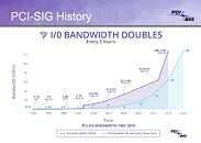
Cadence Design Systems, Inc. (Nasdaq: CDNS) today announced that its PHY and Controller IP for the PCI Express (PCIe ) 5.0 specification in the TSMC N7, N6 and N5 process technologies have passed certification tests from PCI-SIG at the industry's first event for PCIe 5.0 specification compliance held in April. The Cadence solutions were tested to their full potential and complied with the full speed of 32GT/s for PCIe 5.0 technology. The compliance program provides designers with testing procedures to assess that the PCIe 5.0 interfaces on their system-on-chip (SoC) designs will operate as expected.

The Cadence IP for PCIe 5.0 technology consists of a PHY, companion controller and Verification IP (VIP) targeted at SoC designs for very high-bandwidth hyperscale computing, networking and storage applications. With Cadence's PHY and Controller Subsystem for PCIe 5.0 architecture, customers can design extremely power-efficient SoCs while accelerating time to market.

Cadence Digital and Custom/Analog Design Flows Certified by TSMC for Latest N3E and N4P Processes

Cadence Design Systems, Inc. today announced that its digital and custom/analog design flows have been certified for the TSMC N3E and N4P processes, supporting the latest Design Rule Manual (DRM). In addition, Cadence and TSMC delivered N3E and N4P process design kits (PDKs) and design flows to accelerate customer adoption and advance mobile, AI and hyperscale computing design innovation. Joint customers are actively designing with the new N3E and N4P PDKs, and several test chips have already been taped out, which demonstrates how Cadence solutions help customers improve engineering efficiency and maximize the power, performance and area (PPA) benefits offered by the latest TSMC process technologies. The Cadence digital and custom/analog advanced-node solutions support the company's Intelligent System Design strategy, enabling system-on-chip (SoC) design excellence.

Cadence worked closely with TSMC to ensure the digital full flow was optimized for TSMC's advanced N3E and N4P process technologies. The complete RTL-to-GDS flow includes the Cadence Innovus Implementation System, Quantus Extraction Solution, Quantus Field Solver, Tempus Timing Signoff Solution and ECO option, Pegasus Verification System, Liberate Characterization Solution and Voltus IC Power Integrity Solution. Additionally, the Cadence Genus Synthesis Solution and predictive iSpatial technology are enabled for the TSMC N3E and N4P process technologies.

Intel Wins US Government Project to Develop Leading-Edge Foundry Ecosystem

The U.S. Department of Defense, through the NSTXL consortium-based S2MARTS OTA, has awarded Intel an agreement to provide commercial foundry services in the first phase of its multi-phase Rapid Assured Microelectronics Prototypes - Commercial (RAMP-C) program. The RAMP-C program was created to facilitate the use of a U.S.-based commercial semiconductor foundry ecosystem to fabricate the assured leading-edge custom and integrated circuits and commercial products required for critical Department of Defense systems. Intel Foundry Services, Intel's dedicated foundry business launched this year, will lead the work.

"One of the most profound lessons of the past year is the strategic importance of semiconductors, and the value to the United States of having a strong domestic semiconductor industry. Intel is the sole American company both designing and manufacturing logic semiconductors at the leading edge of technology. When we launched Intel Foundry Services earlier this year, we were excited to have the opportunity to make our capabilities available to a wider range of partners, including in the U.S. government, and it is great to see that potential being fulfilled through programs like RAMP-C." -Pat Gelsinger, Intel CEO.

Cadence Announces New Low-Power IP for PCI Express 5.0 Specification on TSMC N5 Process

Cadence Design Systems, Inc. (Nasdaq: CDNS) today announced immediate availability of Cadence IP supporting the PCI Express (PCIe ) 5.0 specification on TSMC N5 process technology. The next follow-on version on TSMC N3 process technology is expected to be taped out in early 2022. Collaboration with major customers is ongoing for N5 SoC designs targeting hyperscale computing and networking applications. The Cadence IP for PCIe 5.0 technology consists of a PHY, companion controller and Verification IP (VIP) targeted at SoC designs for very high-bandwidth hyperscale computing, networking and storage applications. With Cadence's PHY and Controller Subsystem for PCIe 5.0 architecture, customers can design extremely power-efficient SoCs with accelerated time to market.

The Cadence IP for PCIe 5.0 architecture offers a highly power-efficient implementation of the standard, with several evaluations from leading customers indicating it provides industry best-in-class power at the maximum data transfer rate of 32GT/s and worst-case insertion loss. Leveraging Cadence's existing N7/N6 silicon validated offering, the N5 design provides a full 512GT/s (gigatransfers per second) power-optimized solution across the full range of operating conditions with a single clock lane.

DDR5 Arrives at 4800 MT/s Speeds, First SoCs this Year

Cadence, a fabless semiconductor company focusing on the development of IP solutions and IC design and verification tools, today posted an update regarding their development efforts for the 5th generation of DDR memory which is giving us some insights into the development of a new standard. The new DDR5 standard is supposed to bring better speeds and lower voltages while being more power-efficient. In the Cadence's blog called Breakfast Bytes, one of Cadence's memory experts talked about developments of the new standards and how they are developing the IP for the upcoming SoC solutions. Even though JEDEC, a company developing memory standards, hasn't officially published DDR5 standard specifications, Cadence is working closely with them to ensure that they stay on track and be the first on the market to deliver IP for the new standard.

Marc Greenberg, a Cadence expert for memory solutions was sharing his thoughts in the blog about the DDR5 and how it is progressing. Firstly, he notes that DDR5 is going to feature 4800 MT/s speeds at first. The initial speeds will improve throughout the 12 months when the data transfer rate will increase in the same fashion we have seen with previous generation DDR standards. Mr. Greenberg also shared that the goals of DDR5 are to have larger memory dies while managing latency challenges, same speed DRAM core as DDR4 with a higher speed I/O. He also noted that the goal of the new standard is not the bandwidth, but rather capacity - there should be 24Gb of memory per die initially, while later it should go up to 32Gb. That will allow for 256 GB DIMMs, where each byte can be accessed under 100 ns, making for a very responsive system. Mr. Greenberg also added that this is the year of DDR5, as Cadence is receiving a lot of orders for their 7 nm IP which should go in production systems this year.
Cadence DDR5

Cadence, Micron Update on DDR5: Still On Track, 1.36x Performance Increase Over DDR4 at Same Data Rate

DDR5 will be the next step in DDR5 memory tech, again bringing increased transfer speeds over the previous JEDEC (the standards body responsible for the DDR specifications) specification. The new memory technology will also bring the customary reductions in operating voltage - the new version will push the 64-bit link down to 1.1V and burst lengths to 16 bits from 1.2V and 8 bits. In addition, DDR5 lets voltage regulators ride on the memory card rather than the motherboard. CPU vendors are also expected to expand the number of DDR channels on their processors from 12 to 16, which could drive main memory sizes to 128 GB from 64 GB today.

DDR5 is being developed with particular attention to the professional environment, where ever-increasingly gargantuan amounts of addressable memory are required. One of the guiding principles over DDR5's development is a density increase (to allow 16 Gbit chips) that would allow for larger volumes of memory (and thus data processing) in the environments that need that. Reduced power consumption also plays a role here, but all of this will have a cost: latency. For end-users, though, this increased latency will be offset by the usual suspects (DDR memory companies such as Crucial, Corsair, just to name some started with the letter C) in tighter timings and increased operating frequencies. JEDEC's specification for DDR5 is set at 4800 MT/s, but it's expected the memory tech will scale to 6400 MT/s, and you know overclocking and performance-focused companies will walk all over the standard.

Cadence and Micron Demo DDR5-4400 Memory Module

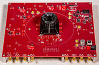
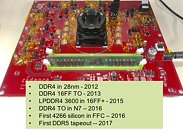
Cadence and Micron have joined forces to build the world's first working DDR5-4400 memory module. Cadence provided their DDR5 memory controller and PHY for the prototype while Micron produced the 8 Gb chips, which were manufactured under TSMC's 7 nm process. They were able to achieve 4400 megatransfers per second, which is roughly 37.5% faster than the fastest DDR4 memory that is currently on the market. Nevertheless, Marc Greenberg from Cadence emphasized that DDR5 aims to provide increased capacity solutions, more than actual performance.

The DDR5 standard should facilitate the production of 16 Gb dies and make vertical stacking easier. Restricted by laws of physics, dies eventually get slower as they increased in size. Once you start putting 16Gb die in 1X memory technology, the distances between them starts to get longer. As a result, core timing parameters become worse. Cadence's prototype had a CAS latency of 42 (No, not a typo). Although, the test module does run at 1.1 volts, which makes it quite impressive when compared to DDR4.

Cadence and Intel Collaborate to Enable a 14 nm Tri-gate Design Platform

Cadence Design Systems, Inc., a leader in global electronic design automation, and Intel Corporation, a world leader in computing innovation, today announced that the companies are collaborating to support Intel's 14 nm Tri-Gate process technology to enable customers of Intel Custom Foundry.

Cadence and Intel have together enabled the custom/analog flow, including Spectre APS, Virtuoso Schematic Editor, Virtuoso Layout Suite and Virtuoso Analog Design Environment for the 14nm Tri-Gate process. The companies are also collaborating on the development of the Cadence digital flow featuring Encounter Digital Implementation System, QRC Extraction Solution, and Tempus Timing Signoff Solution. Using these design flows, customers can leverage the power, performance and area benefits of Intel's 14 nm process technology.

TSMC and Cadence Strengthen Collaboration on 16 nm FinFET Process Development

Cadence Design Systems, Inc., today announced an ongoing multi-year agreement with TSMC to develop the design infrastructure for 16-nanometer FinFET technology, targeting advanced node designs for mobile, networking, servers and FPGA applications. The deep collaboration, beginning earlier in the design process than usual, will effectively address the design challenges specific to FinFETs -- from design analysis through signoff -- and will deliver the infrastructure necessary to enable ultra low-power, high-performance chips.

FinFETs help deliver the power, performance, and area (PPA) advantages that are needed to develop highly differentiated SoC designs at 16 nanometers and smaller process technologies. Unlike a planar FET, the FinFET employs a vertical fin-like structure protruding from the substrate with the gate wrapping around the sides and top of the fin, thereby producing transistors with low leakage currents and fast switching performance. This extended Cadence-TSMC collaboration will produce the design infrastructure that chip designers need for accurate electrical characteristics and parasitic models required for advanced FinFET designs for mobile and enterprise applications.

Cadence Announces Tapeout of 14 nm Test-Chip

Cadence Design Systems, Inc., a leader in global electronic design innovation, announced today the tapeout of a 14-nanometer test-chip featuring an ARM Cortex-M0 processor implemented using IBM's FinFET process technology. The successful tapeout is the result of close collaboration between the three technology leaders as they teamed to build an ecosystem to address the new challenges from design through manufacturing inherent in a 14-nanometer FinFET-based design flow.

The 14-nanometer ecosystem and chip are significant milestones of a multi-year agreement between ARM, Cadence and IBM to develop systems-on-chip (SoCs) at the advanced process nodes of 14 nanometers and beyond. SoCs designed at 14 nanometers with FinFET technology offer the promise of a significant reduction in power consumption.

TSMC Selects Cadence Virtuoso and Encounter Platforms for 20 nm Design Infrastructure

Cadence Design Systems, Inc., a leader in global electronic design innovation, announced today that TSMC has selected Cadence solutions for its 20-nanometer design infrastructure. The solutions cover the Virtuoso custom/analog and Encounter RTL-to-signoff platforms.

The TSMC 20-nanometer reference flows incorporate new features and methodologies in both Encounter and Virtuoso that take into account newly important wire characteristics, timing closure and design size considerations.
Return to Keyword Browsing
May 1st, 2024 00:25 EDT change timezone

New Forum Posts

Popular Reviews

Controversial News Posts