News Posts matching #DDR5

Return to Keyword Browsing

Intel Alder Lake-S CPU Has Been Pictured

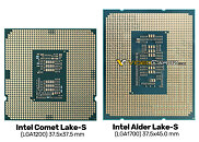
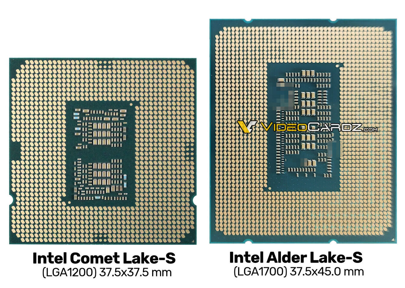
Intel has been preparing the launch of its 10 nm processors for desktop users for some time now, and today we are getting the first pictures of the Alder Lake-S CPU backside. Featuring a package with a size of 37.5×45 mm, the Alder Lake CPU uses more of its area for a pin count increase. Going up from 1200 pins in the LGA1200 socket, the new Alder Lake-S CPU uses 1700 CPU pins, which slots in the LGA1700 socket. In the picture below, there is an engineering sample of the Alder Lake-S CPU, which we see for the first time. While there is no much information about the processor, we know that it will use Intel's 10 nm SuperFin design, paired with hybrid core technology. That means that there will be big (Golden Cove) and little (Gracemont) cores in the design. Other features such as PCIe 5.0 and DDR5 should be present as well. The new CPU generation and LGA1700 motherboards are scheduled to arrive in second half of 2021.

SK hynix Launches World's First DDR5 DRAM

SK hynix Inc. announced to launch world's first DDR5 DRAM. It is a high-speed and high-density product optimized for Big Data, Artificial Intelligence (AI), and machine learning (ML) as a next generation standard of DRAM. Since SK hynix announced the development of World's First 16 Gigabit (Gb) DDR5 DRAM on November 2018, the Company has provided its major partners including Intel with sample products, and has completed various tests and verification of its functions and compatibility. This will allow SK hynix to provide its customers with the products once the DDR5 market becomes active.

In the meantime, SK hynix has conducted joint-operation of on-site lab, system-level test, and simulation with System-on-Chip) (SoC) manufacturers to verify the functions of DDR5. Also, the Company validated compatibility of its DDR5 and the major components on DRAM module including register clock driver) (RCD), which affect DRAM performance, and power management integrated circuit) (PMIC). Through these verifications, SK hynix has been collaborating closely with its global partners.

Intel 11th Gen Core "Tiger Lake" & Xe Graphics Launch Event: Live Blog

Intel today launches its 11th Gen Core "Tiger Lake" mobile processors that introduce several new technologies on the backs of new IP. As described in the Architecture Day, "Tiger Lake" is built on the 10 nm SuperFin process, and combines new "Willow Cove" CPU cores with the first commercial debut of the Xe Gen12 graphics architecture that Intel is betting big on, to make a stab at the consumer graphics and scalar compute markets. Join us in this live-blog.

Update 16:00 UTC: GB (Gregory Bryant, EVP Client), leads the event from the comfort of his home.
Update 16:04 UTC: Here it is, the "world's best processor for thin and light laptops. You'll notice that like most Intel U-segment chips, this is an MCM of the processor and PCH die. Intel bases its "world's best" claims on a per-segment basis.

Intel "Willow Cove" Core, Xe LP iGPU, and "Tiger Lake" SoC Detailed

A lot is riding for Intel on its 11th Gen Core "Tiger Lake" system-on-chip (SoC), which will launch exclusively on mobile platforms, hoping to dominate the 7 W thru 15 W ultraportable form-factors in 2020, while eventually scaling up to the 25 W thru 45 W H-segment form-factors in 2021, with a variant that is rumored to double core-counts. The chip is built on Intel's new 10 nm SuperFin silicon fabrication node that enables a double digit percentage energy efficiency growth over 10 nm, allowing Intel to significantly dial up clock speeds without impacting the power envelope. The CPU and iGPU make up the two key components of the "Tiger Lake" SoC.

The CPU component on the "Tiger Lake" processors that launch in a few weeks from now features four "Willow Cove" CPU cores. Coupled with HyperThreading, this ends up being a 4-core/8-thread setup, although much of Intel's innovation is in giving these cores significant IPC increases over the "Skylake" core powering "Comet Lake" processors, and compared to the "Sunny Cove" cores powering "Ice Lake" a minor IPC (although major net performance increase from clock speeds). The "Willow Cove" CPU core appears to be a derivative of the "Sunny Cove" core, designed to take advantage of the 10 nm SuperFin node, along with three key innovations.

SK hynix Inc. Reports Second Quarter 2020 Results

SK hynix Inc. today announced financial results for its second quarter 2020 ended on June 30, 2020. The consolidated revenue of second quarter 2020 was 8.607 trillion won while the operating profit amounted to 1.947 trillion won, and the net income 1.264 trillion won. Operating margin for the quarter was 23% and net margin was 15%.

Despite uncertainties of business environment due to COVID-19, both the Company's revenue and operating income increased by 20% and 143% quarter-over-quarter (QoQ) respectively, as the surging demand for server memory maintained favorable memory price while numerous factors including the increase of the main products' yield rate led to cost reduction.

JEDEC Publishes New DDR5 Standard for Advancing Next-Generation High Performance Computing Systems

JEDEC Solid State Technology Association, the global leader in the development of standards for the microelectronics industry, today announced the publication of the widely-anticipated JESD79-5 DDR5 SDRAM standard. The standard addresses demand requirements being driven by intensive cloud and enterprise data center applications, providing developers with twice the performance and much improved power efficiency. JESD79-5 DDR5 is now available for download from the JEDEC website.

DDR5 was designed to meet increasing needs for efficient performance in a wide range of applications including client systems and high-performance servers. DDR5 incorporates memory technology that leverages and extends industry know-how and experience developing previous DDR memories. The standard is architected to enable scaling memory performance without degrading channel efficiency at higher speeds, which has been achieved by doubling the burst-length to BL16 and bank-count to 32 from 16. This revolutionary architecture provides better channel efficiency and higher application level performance that will enable the continued evolution of next-generation computing systems. In addition, the DDR5 DIMM has two 40-bit fully independent sub-channels on the same module for efficiency and improved reliability.

New features, such as DFE (Decision Feedback Equalization), enable IO speed scalability for higher bandwidth and improved performance. DDR5 supports double the bandwidth as compared to its predecessor, DDR4, and is expected to be launched at 4.8 Gbps (50% higher than DDR4's end of life speed of 3.2 Gbps).

Micron Drives DDR5 Adoption With Technology Enablement Program

Micron Technology, Inc., today announced a comprehensive enablement program which will provide early access to technical resources, products and ecosystem partners. The Technology Enablement Program will aid in the design, development and qualification of next-generation computing platforms that use DDR5, the most technologically advanced DRAM available.

Today's news builds on Micron's January announcement of DDR5 RDIMM samples and brings the industry one step closer to unlocking the value in next-generation, data-centric applications. Companies joining Micron in the DDR5 Technology Enablement Program include Cadence, Montage, Rambus, Renesas and Synopsys.

Distant Blips on the AMD Roadmap Surface: Rembrandt and Raphael

Several future AMD processor codenames across various computing segments surfaced courtesy of an Expreview leak that's largely aligned with information from Komachi Ensaka. It does not account for "Matisse Refresh" that's allegedly coming out in June-July as three gaming-focused Ryzen socket AM4 desktop processors; but roadmap from 2H-2020 going up to 2022 sees many codenames surface. To begin with, the second half of 2020 promises to be as action packed as last year's 7/7 mega launch. Over in the graphics business, the company is expected to debut its DirectX 12 Ultimate-compliant RDNA2 client graphics, and its first CDNA architecture-based compute accelerators. Much of the processor launch cycle is based around the new "Zen 3" microarchitecture.

The server platform debuting in the second half of 2020 is codenamed "Genesis SP3." This will be the final processor architecture for the SP3-class enterprise sockets, as it has DDR4 and PCI-Express gen 4.0 I/O. The EPYC server processor is codenamed "Milan," and combines "Zen 3" chiplets along with an sIOD. EPYC Embedded (FP6 package) processors are codenamed "Grey Hawk."

Intel "Alder Lake" LGA1700 to Feature DDR5; "Rocket Lake" Thermal Specs Leaked

PTT leaked some juicy details of the upcoming Intel "Rocket Lake" and "Alder Lake" processor generations. "Rocket Lake" will power Intel's 11th generation Core processor series in the LGA1200 package, and are rumored to be a "back port" of Intel's advanced "Willow Cove" CPU cores to a 14 nm-class silicon fabrication node, with core-counts ranging up to 8. The idea for Intel is to sell high IPC, high clock-speed desktop processors for gaming.

According to the PTT report, there will be three kinds of SKUs for "Rocket Lake" based on TDP: 8-core parts with 95 W TDP rating; and 8-core, 6-core, and 4-core parts in 80 W TDP and 65 W TDP variants. For the 95 W (PL1) parts, the power-levels PL2, and PL4 are reportedly set at 173 W and 251 W, respectively, and a 56-second Tau (a timing variable that dictates how long a processor can stick around at an elevated power-state before retreating to PL1, which is interchangeable with the TDP value on the box). The 80 W TDP parts feature 146 W PL2, 191 W PL3, and 251 W PL4, but a lower Tau value of 28 seconds. For the 65 W parts, the PL2 is 128 W, PL3 is 177 W, and PL4 251 W, and the Tau value 28 seconds.

Tachyum Achieves 90 Percent of Silicon Laid for its Prodigy Universal Processor

Semiconductor startup Tachyum Inc. announced today that it has achieved, on schedule, a major milestone in the detailed physical design of its Prodigy Universal Processor. Tachyum now has a complete chip layout, with a verified detailed physical design of more than 90 percent of the design silicon area.

Tachyum's Prodigy is the world's first Universal Processor, combining general-purpose processors, high-performance computing (HPC), artificial intelligence (AI), deep machine learning (ML), explainable AI, bio AI and other AI disciplines within a single chip. This latest milestone achieved integration of key, high-quality Tachyum IP within a multiprocessor environment, and with DDR4/DDR5 DRAM controllers, PCIE 5.0, 112Gb SERDES, USB, GPIO, PLLs and various I/Os. Results of the layout indicate that Prodigy's die size is within product design goals with top-level clocking results that are better than expected.

Tachyum Prodigy is a Small 128-core Processor with Crazy I/O Options, 64-core Sibling Enroute Production

Silicon Valley startup Tachyum, founded in 2016, is ready with its crowning product, the Tachyum Prodigy. The startup recently received an investment from the Slovak government in hopes of job-creation in the country. The Prodigy is what its makers call "a universal processor," which "outperforms the fastest Xeon at 10X lower power." The company won't mention what machine architecture it uses (whether it's Arm or MIPS, or its own architecture). Its data-sheet is otherwise full of specs that scream at you.

To begin with, its top trim, the Prodigy T16128, packs 128 cores on a single package, complete with 64-bit address space, 512-bit vector extensions, matrix multiplication fixed-function hardware that accelerate AI/ML, and 4 IPC at up to 4.00 GHz core clock. Tachyum began the processor's software-side support, with an FPGA emulator in December 2019 (so you can emulate the processor on an FPGA and begin developing for it), C/C++ and Fortran compilers; debuggers and profilers, tensorflow compilers, and a Linux distribution that's optimized it. The I/O capabilities of this chip are something else.

AMD to Support DDR5, LPDDR5, and PCI-Express gen 5.0 by 2022, Intel First to Market with DDR5

AMD is expected to support the next-generation DDR5 memory standard by 2022, according to a MyDrivers report citing industry sources. We are close to a change in memory standards, with the 5-year old DDR4 memory standard beginning a gradual phase out over the next 3 years. Leading DRAM manufacturers such as SK Hynix have already hinted mass-production of the next-generation DDR5 memory to commence within 2020. Much like with DDR4, Intel could be the first to market with processors that support it, likely with its "Sapphire Rapids" Xeon processors. AMD, on the other hand, could debut support for the standard only with its "Zen 4" microarchitecture slated for 2021 technology announcements, with 2022 availability.

AMD "Zen 4" will see a transition to a new silicon fabrication process, likely TSMC 5 nm-class. It will be an inflection point for the company from an I/O standpoint, as it sees the introduction of DDR5 memory support across enterprise and desktop platforms, LPDDR5 on the mobile platform, and PCI-Express gen 5.0 across the board. Besides a generational bandwidth doubling, PCIe gen 5.0 is expected to introduce several industry-standard features that help with hyper-scalability in the enterprise segment, benefiting compute clusters with multiple scalar processors, such as AMD's CDNA2. Intel introduced many of these features with its proprietary CXL interconnect. AMD's upcoming "Zen 3" microarchitecture, scheduled for within 2020 with market presence in 2021, is expected to stick with DDR4, LPDDR4x, and PCI-Express gen 4.0 standards. DDR5 will enable data-rates ranging between 3200 to 8400 MHz, densities such as single-rank 32 GB UDIMMs, and a few new physical-layer features such as same-bank refresh.

Micron's Low-Power DDR5 DRAM Boosts Performance and Consumer Experience of Motorola's New Flagship Edge+ Smartphone

Micron Technology, Inc., together with Motorola, today announced integration of Micron's low-power DDR5 (LPDDR5) DRAM into Motorola's new motorola edge+ smartphone, bringing the full potential of the 5G experience to consumers. Micron and Motorola worked in close collaboration to enable the edge+ to reach 5G network speeds that require maximum processing power coupled with high bandwidth memory and storage.

With 12 gigabytes (GB) of industry-leading Micron LPDDR5 DRAM memory, motorola edge+ delivers a smooth, lag-free consumer experience. The new phone takes advantage of the faster data speeds and lower latency of 5G to increase the performance of cloud-based applications such as gaming and streaming entertainment.
Motorola Edge+

SK Hynix Unveils DDR5 Memory Details, Production to Start This Year

SK Hynix has today posted an update on their blog about the upcoming DDR5 memory, which they have developed in co-respondence with JEDEC's progression of the standard. They have noted a few key things, among which some of the most interesting are features like the maximum speed of 8400 Mbps. The DDR5 standard is very flexible, allowing manufacturers to release their chips with frequencies ranging anywhere from 3200-8400 Mbps. While the lowest speed is 3200 Mbps, manufacturers are starting with 4800 Mbps chips and building their way up from there. The minimum density of a single DDR5 die is 8 Gb, while the maximum is 64 Gb, quadrupling the maximum capacity of DDR4 dies.

Perhaps one of the biggest changes besides capacity and speed improvements is the addition of Error-Correcting Code (ECC) support for memory. This feature is now not exclusive to special dies, like with DDR4, but rather is built inside every die. The DDR5 memory chips use 32 banks, split into 8 bank groups, which is designed to provide as much bandwidth as possible. Burst Length is doubled to 16, compared to 8 of DDR4, so memory access availability is better. Operating Voltage is decreased to 1.1 V, from the previous 1.2 V of DDR4, resulting in an overall decrease of 20% of power consumption. The mass production of SK-Hynix's DDR5 chips will start this year, however, exact timing is unknown.
SK Hynix DDR5 SK Hynix DDR5 SK Hynix DDR5

DDR5 Arrives at 4800 MT/s Speeds, First SoCs this Year

Cadence, a fabless semiconductor company focusing on the development of IP solutions and IC design and verification tools, today posted an update regarding their development efforts for the 5th generation of DDR memory which is giving us some insights into the development of a new standard. The new DDR5 standard is supposed to bring better speeds and lower voltages while being more power-efficient. In the Cadence's blog called Breakfast Bytes, one of Cadence's memory experts talked about developments of the new standards and how they are developing the IP for the upcoming SoC solutions. Even though JEDEC, a company developing memory standards, hasn't officially published DDR5 standard specifications, Cadence is working closely with them to ensure that they stay on track and be the first on the market to deliver IP for the new standard.

Marc Greenberg, a Cadence expert for memory solutions was sharing his thoughts in the blog about the DDR5 and how it is progressing. Firstly, he notes that DDR5 is going to feature 4800 MT/s speeds at first. The initial speeds will improve throughout the 12 months when the data transfer rate will increase in the same fashion we have seen with previous generation DDR standards. Mr. Greenberg also shared that the goals of DDR5 are to have larger memory dies while managing latency challenges, same speed DRAM core as DDR4 with a higher speed I/O. He also noted that the goal of the new standard is not the bandwidth, but rather capacity - there should be 24Gb of memory per die initially, while later it should go up to 32Gb. That will allow for 256 GB DIMMs, where each byte can be accessed under 100 ns, making for a very responsive system. Mr. Greenberg also added that this is the year of DDR5, as Cadence is receiving a lot of orders for their 7 nm IP which should go in production systems this year.
Cadence DDR5

Samsung Announces Industry's First EUV DRAM with Shipment of First Million Modules

Samsung Electronics Co., Ltd., the world leader in advanced memory technology, today announced that it has successfully shipped one million of the industry's first 10 nm-class (D1x) DDR4 (Double Date Rate 4) DRAM modules based on extreme ultraviolet (EUV) technology. The new EUV-based DRAM modules have completed global customer evaluations, and will open the door to more cutting-edge EUV process nodes for use in premium PC, mobile, enterprise server and datacenter applications.

"With the production of our new EUV-based DRAM, we are demonstrating our full commitment toward providing revolutionary DRAM solutions in support of our global IT customers," said Jung-bae Lee, executive vice president of DRAM Product & Technology at Samsung Electronics. "This major advancement underscores how we will continue contributing to global IT innovation through timely development of leading-edge process technologies and next-generation memory products for the premium memory market."
Samsung EUV DDR4

Micron Samples the Industry's First uMCP Product With LPDDR5 to Increase Performance and Battery Life in 5G Smartphones

Micron Technology, Inc., today announced it began sampling the industry's first universal flash storage (UFS) multichip package (uMCP) with low-power DDR5 (LPDDR5) DRAM. The uMCP provides high-density and low-power storage designed to fit on slim and compact midrange smartphone designs.

Micron's new uMCP5 packaging builds on the company's innovation and leadership in multichip form factors. Micron uMCPs combine low-power DRAM with NAND and an onboard controller, using 40% less space compared to a two-chip solution. This optimized configuration saves power, reduces memory footprint and enables smaller and more agile smartphone designs.
RAM Production

Micron Ships World's First LPDDR5 DRAM for High-Performance Smartphones

Micron Technology, Inc., today announced it has shipped the world's first low-power DDR5 DRAM in mass production to be used in the soon-to-be-released Xiaomi Mi 10 smartphone. As Xiaomi's memory technology partner, Micron provides LPDDR5 DRAM with superior power efficiency and faster data access speeds to meet growing consumer demand for artificial intelligence (AI) and 5G functionality in smartphones.

"Micron's leadership in delivering the industry's first low-power DDR5 DRAM for use in a smartphone will accelerate enablement of 5G and AI applications," said Dr. Raj Talluri, senior vice president and general manager of the Mobile Business Unit at Micron. "Our customers and partners require next-generation memory solutions, based on the latest process technology, that drive unmatched power and performance to support 5G and AI systems. Micron's LPDDR5 DRAM addresses those requirements with a 50% increase in data access speeds and more than 20% power efficiency compared to previous generations."

"We value Micron's long-standing leadership and innovation in memory," said Chang Cheng, vice president at Xiaomi Group. "Micron's LPDDR5 DRAM market-leading features ensure our Xiaomi Mi 10 smartphone will remain power-efficient while still offering incredible performance and greater stability. We believe LPDDR5 will be the standard configuration for all flagship devices in 2020."

Europe Readies its First Prototype of Custom HPC Processor

European Processor Initiative (EPI) is a Europe's project to kickstart a homegrown development of custom processors tailored towards different usage models that the European Union might need. The first task of EPI is to create a custom processor for high-performance computing applications like machine learning, and the chip prototypes are already on their way. The EPI chairman of the board Jean-Marc Denis recently spoke to the Next Platform and confirmed some information regarding the processor design goals and the timeframe of launch.

Supposed to be manufactured on TSMC's 6 nm EUV (TSMC N6 EUV) technology, the EPI processor will tape-out at the end of 2020 or the beginning of 2021, and it is going to be heterogeneous. That means that on its 2.5D die, many different IPs will be present. The processor will use a custom ARM CPU, based on a "Zeus" iteration of Neoverese server core, meant for general-purpose computation tasks like running the OS. When it comes to the special-purpose chips, EPI will incorporate a chip named Titan - a RISC-V based processor that uses vector and tensor processing units to compute AI tasks. The Titan will use every new standard for AI processing, including FP32, FP64, INT8, and bfloat16. The system will use HBM memory allocated to the Titan processor, have DDR5 links for the CPU, and feature PCIe 5.0 for the inner connection.

SK hynix Displays its Semiconductor Technologies Leading the 4th Industrial Revolution

SK hynix Inc. presents its innovative semiconductor technologies leading the 4th Industrial Revolution at CES 2020, the world's largest trade show for IT and consumer electronics in Las Vegas, USA, from January 7-10, 2020. In line with its "Memory Centric World" theme, SK hynix depicts a futuristic city which effectively utilizes enormous amounts of data. The Company also showcases its semiconductor solutions across six crucial business fields - artificial intelligence (AI), augmented reality (AR) / virtual reality (VR), automotive, Internet of Things (IoT), big data and 5G.

Headlining at CES 2020 are SK hynix's memory solutions including HBM2E, DDR5 for servers, and SSD, which are already highly regarded and widely used in 4th industrial fields such as 5G and AI for their stability, speed, power consumption and density excellence. Other cutting-edge products set to make headlines in January are the Company's highly durable LPDDR4X and eMMC 5.1, which are optimized for automobiles. What's more, SK hynix is displaying its LPDDR5 and UFS that enhance the performance of 5G smartphones as well as CIS (CMOS Image Sensor) which is essential in establishing effective environments for AR/VR and IoT.

Micron Start Sampling DDR5 RDIMMs

Micron has today announced that it started sampling RDIMMs based on DDR5 technology to its industry partners. Designed for server operations, these DDR5 modules come in RDIMM form-factor and feature Error-Correcting Code (ECC) technology for removing any error that occurs inside electronic circuits. The new DDR5 standard offers a massive performance uplift compared to the previous generation of DDR4 memory. For starters, DDR5 will double the MT/s transfer rate to 6400 MT/s, double the speed of the original 3200 MT/s speed for DDR4 that was established by JEDEC. The bandwidth of the new DDR memory is supposed to be 32 GB/s, which is 25% faster than the original 25.6 GB/s bandwidth of DDR4.

With DDR5, the SDRAM prefetch buffer data size is being doubled to 16 data words per memory access, making for a 16n prefetching throughput. Another improvement is that the highest possible density for DDR5 chips is now being up to 64 Gb per chip. Additionally, DDR5 is supposed to bring the power needed for chip operation down to 1.1 volts, which is around 8% lower than what DDR4 achieved. There are also features like MIR (Mirror Pin) which provides better DIMM signaling, and more options for PRECHARGE and REFRESH commands that can now operate on a per bank basis, so specific banks can be refreshed in bank group. It is also worth pointing out that DDR5 chips are manufactured using 1znm memory manufacturing process.

Intel "Tiger Lake-U" Processors Could Support LPDDR5 Memory

Intel's Core "Tiger Lake" microarchitecture could be a point of transition between DDR4 and DDR5 for the company. Prototypes of devices based on the ultra-compact "Tiger Lake-Y" SoC were earlier shown featuring LPDDR4X memory, although a new device, possibly a prototyping platform, in the regulatory queue with the Eurasian Economic Commission describes itself as featuring a "Tiger Lake-U" chip meant for thin and light notebooks and convertibles. This device features newer LPDDR5 memory, according to its regulatory filing.

LPDDR5 succeeds LPDDR4X as the industry's next low-power memory standard, offering data-rates of up to 6,400 MT/s (versus up to 4,266 MT/s of LPDDR4X), and consumes up to 30 percent less power. This prototype at the EEC is sure to be using unreleased LPDDR5 memory chips as DRAM majors Samsung and SK Hynix plan to ship their DDR5-based memory solutions only by the end of this year, although mass-production of the chips have already started at Samsung, in PoP form-factors. A successor to the 10th generation Core "Ice Lake," "Tiger Lake" will be Intel's second CPU microarchitecture designed for its 10 nm silicon fabrication node.

Intel Ships First 10nm Agilex FPGAs

Intel today announced that it has begun shipments of the first Intel Agilex field programmable gate arrays (FPGAs) to early access program customers. Participants in the early access program include Colorado Engineering Inc., Mantaro Networks, Microsoft and Silicom. These customers are using Agilex FPGAs to develop advanced solutions for networking, 5G and accelerated data analytics.

"The Intel Agilex FPGA product family leverages the breadth of Intel innovation and technology leadership, including architecture, packaging, process technology, developer tools and a fast path to power reduction with eASIC technology. These unmatched assets enable new levels of heterogeneous computing, system integration and processor connectivity and will be the first 10nm FPGA to provide cache-coherent and low latency connectivity to Intel Xeon processors with the upcoming Compute Express Link," said Dan McNamara, Intel senior vice president and general manager of the Networking and Custom Logic Group.

Samsung Begins Mass Production of Industry's First 12Gb LPDDR5 Mobile DRAM

Samsung Electronics, the world leader in advanced memory technology, today announced that it has begun mass producing the industry's first 12-gigabit ( Gb) LPDDR5 mobile DRAM, which has been optimized for enabling 5G and AI features in future smartphones. The new mobile memory comes just five months after announcing mass production of the 12 GB LPDDR4X, further reinforcing the company's premium memory lineup. Samsung also plans to start mass producing 12-gigabyte (GB) LPDDR5 packages later this month, each combining eight of the 12 Gb chips, in line with growing demand for higher smartphone performance and capacity from premium smartphone manufacturers.

"With mass production of the 12 Gb LPDDR5 built on Samsung's latest second-generation 10-nanometer (nm) class process, we are thrilled to be supporting the timely launch of 5G flagship smartphones for our customers worldwide," said Jung-bae Lee, executive vice president of DRAM Product & Technology, Samsung Electronics. "Samsung remains committed to rapidly introducing next-generation mobile memory technologies that deliver greater performance and higher capacity, as we continue to aggressively drive growth of the premium memory market."

Intel "Sapphire Rapids" Brings PCIe Gen 5 and DDR5 to the Data-Center

As if the mother of all ironies, prior to its effective death-sentence dealt by the U.S. Department of Commerce, Huawei's server business developed an ambitious product roadmap for its Fusion Server family, aligning with Intel's enterprise processor roadmap. It describes in great detail the key features of these processors, such as core-counts, platform, and I/O. The "Sapphire Rapids" processor will introduce the biggest I/O advancements in close to a decade, when it releases sometime in 2021.

With an unannounced CPU core-count, the "Sapphire Rapids-SP" processor will introduce DDR5 memory support to the data-center, which aims to double bandwidth and memory capacity over the DDR4 generation. The processor features an 8-channel (512-bit wide) DDR5 memory interface. The second major I/O introduction is PCI-Express gen 5.0, which not only doubles bandwidth over gen 4.0 to 32 Gbps per lane, but also comes with a constellation of data-center-relevant features that Intel is pushing out in advance as part of the CXL Interconnect. CXL and PCIe gen 5 are practically identical.
Return to Keyword Browsing
May 21st, 2024 21:58 EDT change timezone

New Forum Posts

Popular Reviews

Controversial News Posts