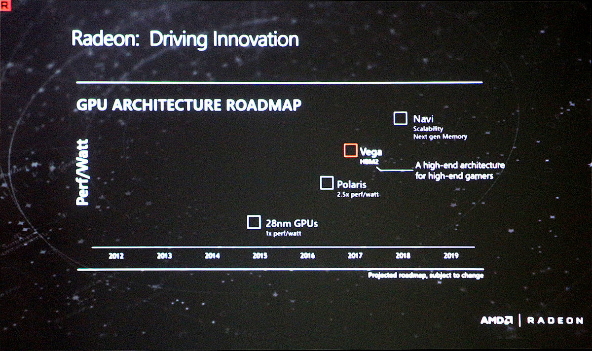
Micron's Outlook for the Future of Memory: GDDR6, QuantX in 2017
After finally reaching mature yields (comparable to those of planar NAND processes), Micron's 32-layer first generation 3D NAND has grown increasingly prominent in the company's NAND output. Now, the company is looking to ramp-up production of their (currently sampling) 64-layer 3D NAND, promising "meaningful output" by the end of December 2017, looking for an 80% increase in total GB per wafer and a 30% decrease in production costs.
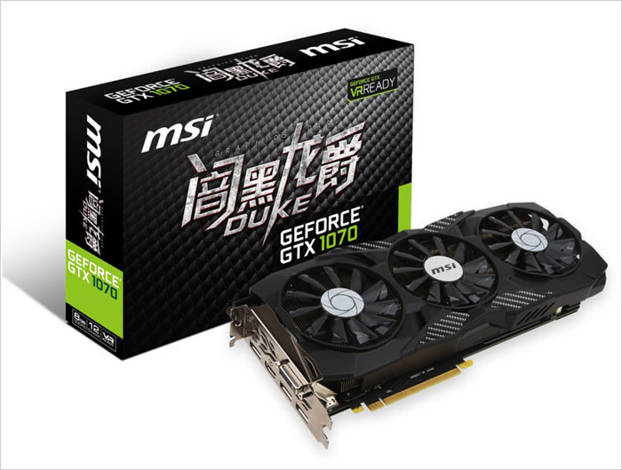
When it comes to the graphics subsystem memory, Micron is looking to transition their 20nm production to a "1x nm" (most likely 16nm) node, in a bid to improve cost per GB by around $20, with introduction of 16nm GDDR5 memory to be introduced later this year. However, GDDR5X volume is expected to grow significantly, in a bid to satisfy bandwidth-hungry uses through GPUs (like NVIDIA's GTX 1080 and potentially the upcoming 1080 Ti) and networking, with GDDR6 memory being introduced by the end of 2017 or early 2018. The company is still mum on actual consumer products based on their interpretation of the 3D XPoint products through their QuantX brand, though work is already under way on the second and third generation specifications of this memory, with Micron planning an hitherto unknown (in significance and product type) presence in the consumer market by the end of this year.

When it comes to the graphics subsystem memory, Micron is looking to transition their 20nm production to a "1x nm" (most likely 16nm) node, in a bid to improve cost per GB by around $20, with introduction of 16nm GDDR5 memory to be introduced later this year. However, GDDR5X volume is expected to grow significantly, in a bid to satisfy bandwidth-hungry uses through GPUs (like NVIDIA's GTX 1080 and potentially the upcoming 1080 Ti) and networking, with GDDR6 memory being introduced by the end of 2017 or early 2018. The company is still mum on actual consumer products based on their interpretation of the 3D XPoint products through their QuantX brand, though work is already under way on the second and third generation specifications of this memory, with Micron planning an hitherto unknown (in significance and product type) presence in the consumer market by the end of this year.