News Posts matching #Global Foundries

Return to Keyword Browsing

GlobalFoundries to Go Public in 2022

GlobalFoundries is planning to sell a minority stake in the company through an IPO (initial public offering) in 2022, company CEO Tom Caulfield told the Wall Street Journal. In February, it was reported that with the discontinuation of the 7 nm development and sale of certain facilities, the perception was made that GloFo was looking to be acquired by another semiconductor company. The same course of actions could have also served as prelude to taking the company public, and as it turns out, GloFo is heading toward the latter.

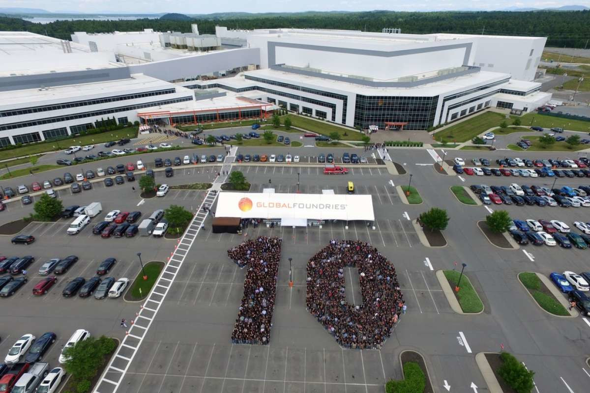
TimesUnion comments that the decision to discontinue 7 nm development and shedding some assets slowed down development of future technologies, but returned the company to profitability, so it could be put up for an IPO. Caulfield didn't comment on what is the size of the stake sale, but the source comments it could be aimed at alleviating the strain on GloFo's original investors, the Abu Dhabi government, which has invested over $21 billion in the company over the past 10 years. GlobalFoundries was formed as AMD spun off its semiconductor business in 2009, with seed capital from the Abu Dhabi government. Over the decade, the company built fabs in New York state, and acquired fabs across Vermont, and Singapore, along with tech acquisition from IBM.

TSMC Files Complaints Against GlobalFoundries for Infringement of 25 Patents

TSMC, the world's leading global innovator in semiconductor manufacturing, filed multiple lawsuits on September 30, 2019 against GlobalFoundries in the United States, Germany and Singapore for its ongoing infringement of 25 TSMC patents by at least its 40nm, 28nm, 22nm, 14nm, and 12nm node processes. In the complaints, TSMC demands injunctions to stop GlobalFoundries' manufacture and sale of infringing semiconductor products. TSMC also seeks substantial monetary damages from GlobalFoundries for its sale of infringing semiconductor products and unlawful use of TSMC's patented semiconductor technologies.

The 25 TSMC patents in the complaints relate to a diverse set of technologies, including FinFET designs, shallow trench isolation techniques, double patterning methods, advanced seal rings and gate structures, and innovative contact etch stop layer designs. These specific technologies cover the core features of mature and advanced semiconductor manufacturing processes. The patents at issue comprise just a small portion of TSMC's extensive portfolio that numbers more than 37,000 granted patents worldwide. TSMC was ranked one of the top 10 companies for U.S. patent grants last year, for the third consecutive year.

Intel Internal Memo Reveals that even Intel is Impressed by AMD's Progress

Today an article was posted on Intel's internal employee-only portal called "Circuit News". The post, titled "AMD competitive profile: Where we go toe-to-toe, why they are resurgent, which chips of ours beat theirs" goes into detail about the recent history of AMD and how the company achieved its tremendous growth in recent years. Further, Intel talks about where they see the biggest challenges with AMD's new products, and what the company's "secret sauce" is to fight against these improvements.
The full article follows:

GlobalFoundries Looking for Buyers, Samsung and SK Hynix Seem Interested

GlobalFoundries is looking to be sold lock-stock-and-barrel by its investors, after heavily downsizing and parting with some of its Singapore-based assets recently. Once promising to lead the market with 7 nm and 5 nm advancements, the company crashed out of the sub-10 nm race, making AMD, its biggest customer, look for 7 nm supplies from TSMC. GlobalFoundries is the world's third largest semiconductor foundry service provider, with an 8.4 percent market share, behind TSMC and Samsung. Intel doesn't offer manufacturing services, as its fabs are fully dedicated to manufacturing its own products.

GlobalFoundries's main investor is Abu Dhabi-based Mubadala Technology, which holds a 90 percent stake in the company. Korean semiconductor companies Samsung and SK Hynix are reportedly in the foray to buy out GlobalFoundries, as it would give them a turnkey presence in the US, with its Upstate New York facilities. The company is unlikely to entertain bids from Chinese companies, as CFIUS would likely block the sale. "Global Foundries is unlikely to be bought by a Chinese company such as SMIC in that the U.S. government is keeping China in check in various industries," said an industry insider, adding, "The most potential candidates include South Korean companies such as Samsung Electronics and SK Hynix, and Samsung Electronics can increase its share in the market to 23 percent at once if it takes over Global Foundries."

GlobalFoundries to Sell its Singapore-based Fab 3E to Vanguard

GlobalFoundries has decided to exit the MEMS (microelectromechanical systems) manufacturing business by selling off its Fab 3E, located in Singapore. The foundry will be acquired lock stock and barrel by Vanguard International Semiconductor (VIS). GlobalFoundries earns USD $236 million from this sale. The transfer of operations is scheduled to take place on 31st December, 2019. Fab 3E has an installed capacity of producing 35,000 200-mm wafers per month, and specializes in MEMS and analog/mixed signal chips. Under the terms of sale, Vanguard also stands to obtain GlobalFoundries' MEMS-related IP and workforce for this facility, which continues its employment after transition. Vanguard also inherits GloFo's clientele for products made at this facility.

AMD Updates Wafer Supply Agreement with GlobalFoundries to Free Itself of "7nm Tax"

AMD in its Q4-2018 Earnings Report disclosed that it has amended its Wafer Supply Agreement (WSA) with GlobalFoundries that frees it from paying a "7 nanometer tax." Under the older version of WSA, AMD would have had to pay a penalty to GlobalFoundries if it sourced processors from any other semiconductor foundry. The company got preferential pricing in return for the exclusivity. With GlobalFoundries discontinuing development of cutting-edge processes such as 7 nm and 5 nm, it makes sense for AMD to seek out other foundry partners, such as TSMC, and an amendment to the WSA was needed. With this amendment in place, AMD can go ahead and source 7 nm dies from TSMC without paying penalties to GlobalFoundries (GloFo).

With its "Zen 2" microarchitecture, AMD is going big on multi-chip modules, in which only those components that can tangibly benefit from the switch to the 7 nm node, namely the CPU cores, would be built on 7 nm dies, called "CPU chiplets," while components that don't need the miniaturization just yet, such as the processor's memory controller, PCIe root-complex, etc., will be built on separate dies called "I/O controllers." These dies will continue to be 14 nm, and likely supplied by GloFo. Final packaging of 7 nm CPU chiplets from TSMC, and 14 nm I/O controllers from GloFo, will happen at GloFo's facilities in China or Malaysia. AMD in its amendment committed to purchasing 14 nm and 12 nm chips from GloFo between 2019 and 2021, which means the MCM approach to processors is here to stay.

GLOBALFOUNDRIES and Chengdu Realign Joint Venture Strategy

GLOBALFOUNDRIES and the Chengdu municipality signed an amendment to their investment and cooperation agreement today. Based on market condition changes, GF's recently announced renewed focus on differentiated offerings, and discussions with potential clients, the partners have decided to bypass the original phase one investment in mainstream process technology (180/130nm). It is also agreed that the project timeline will be adapted to better align capacity to meet China-based demand for differentiated offerings including GF's industry leading 22FDX technology.

With more than $2 billion of design wins and more than 50 client designs, GF's 22FDX technology is demonstrating traction as the industry's leading platform for power-optimized chips across a broad range of high-growth applications such as automotive, 5G connectivity and the Internet of Things (IoT). GF's Chinese clients are beginning to adopt the technology at GF's advanced manufacturing site in Dresden, Germany, including seven customers and more than nine products in various stages of manufacturing ramp.

"We have a long-term relationship with GF and the 22FDX with its low power is very suitable for our various products, including AI and security," said Min Li, CEO of Rockchip. "Once we achieve the right level of readiness, we look forward to ramping our production closer to home in China."

Chances of Intel Going Fabless Higher Than Ever

Intel is one of the few semiconductor companies that manufactures a majority of its products on its own silicon fabrication foundries. The breadwinner for the company continues to be CPUs, and a majority of its revenues continue to come from its client-computing group (CCG). CPUs, like GPUs, are required to be built on the latest silicon fabrication process to keep up (or catch up) with Moore's Law. Intel is plagued with severe technological roadblocks toward advancing its foundry process from 14 nanometer (nm) to its next step, 10 nm. In its latest Q2-2018 earnings call, the company confirmed that the 10 nm node won't put out before Q4-2019, even as rival AMD's CEO announced that its first 7 nm processors will be up for purchase by the end of 2018 (a year ahead with a more advanced process, on paper). Analysts are beginning to paint a very grim future for Intel's foundry business.

The prospects for Intel going fabless, at least for its cutting-edge products, is higher than ever. Analysts, speaking with Taiwan-based industry observer DigiTimes, mentioned that there is speculation of Intel scaling down its foundry business. Something like this, if true, could hint at the company looking for foundry partners with newer silicon-fabrication nodes at a more advanced stage of development (eg: GlobalFoundries 7 nm) to manufacture its processors, while relegating its own foundries to manufacture less complex products such as chipset, NAND flash, 3D XPoint memory, 5G PHYs, etc. Fancy a Core processor made by GloFo in the great state of New York?

AMD to Detail Vega, Navi, Zen+ on May 16th - Laying Out a Vision

Reports are circling around the web regarding an AMD meeting featuring some of its higher ups - namely, CEO Lisa Su, head of Radeon Technologies Group Raja Koduri, and AMD's CTO Mark Papermaster happening on the 16th of May. The purpose of this meeting seems to be to discuss AMD's inflexion point, and lay out a vision for the company's future, supported on its upcoming products: the too-long-awaited Vega, its successor Navi, and the natural evolution of the company's current Zen processors, tentatively identified as Zen+.

Naturally, a company such as AMD has its roadmap planned well in advance, with work on next-generation products and technologies sometimes even running in parallel with current-generation product development. It's just a result of the kind of care, consideration, time and money that goes into making new architectures that makes this so. And while some would say Vega is now approaching a state akin to grapes that have been hanging for far too long, AMD's next graphics architecture, Navi, and its iterations on Zen cores, which the company expect to see refreshes in a 3-to-5-year period, are other matters entirely. Maybe we'll have some more details regarding the specific time of Vega's launch (for now expected on Computex), as well as on when AMD is looking to release a Zen+ refresh. I wouldn't expect much with regards to Navi - perhaps just an outline on how work is currently underway with some comments on the expectations surrounding Global Foundries' 7 nm process, on which Navi is expected to be built. And no, folks, this isn't a Vega launch. Not yet.

AMD Files Patent Infringement Complaint Against LG, Vizio, Others

On January 24, 2017, AMD filed a complaint against several prominent tech companies, requesting that the ITC commence an investigation pursuant to Section 337. The basis for the complaint: some of these companies (namely, LG, MediaTek, VIZIO, and Sigma) unlawfully import into or sell inside the U.S. products which infringe on AMD's graphics intelectual property - namely, on U.S. Patent Nos. 7,633,506 (the '506 patent), 7,796,133 (the '133 patent) and 8,760,454 (the '454 patent) (collectively, the "asserted patents".

According to the complaint, these patents generally relate to architectures for graphics processing unit (GPU) circuitry. The '506 patent relates to "a graphics processing architecture that enables a large amount of graphics data to be rendered to a frame buffer". The '133 patent relates to specialized "texture" processing circuitry that is employed by GPUs. Lastly, the '454 patent relates to a "unified shader" hardware architecture for GPUs. The complaint specifically refers to various televisions and smartphones, specifically, towards the graphics processing systems within those televisions and smartphones - as infringing products.

AMD "Llano" Securities Fraud Lawsuit Ongoing; Class Action Status Granted

As you may remember, "Llano" was somewhat of a disappointment for AMD, to put it mildly. Production issues with partner Global Foundries meant that Llano's roll-out was affected and extended beyond its predicted time-frame. This, in conjunction with other various factors, such as lack of product appeal over disappointing performance and the usual competition from Intel, forced AMD to pull in its second-generation "Trinity" APU too soon. By the time production finally caught up, it ended up overproducing relative to diminishing demand, which resulted in unsold inventory, thus forcing an inventory write-down of "Llano" chips valued at around $100 million. This reduced the company's worth by nearly that much overnight, and tanked the value of the AMD stock. This, of course, didn't sit well with investors.

The as-of-yet ongoing securities fraud lawsuit over AMD's "Llano" APUs has just achieved a milestone, in having been authorized by the Court to proceed as a class action. The Court's decision doesn't imply that the defendants (Rory P. Read, Thomas J. Seifert, Richard A. Bergman, and Dr. Lisa T. Su) did anything wrong. The defendants have not been ordered to pay any money, no settlement has been reached, no money is available as of now and there is no guarantee that there will be in the future.

Engineering Sample Of AMD Steamroller Based APU Spotted

Hardware news site WCCF Tech spotted an interesting entry listed in the Bionic research database. The ES (Engineering Sample) chip could be a part of AMD's next-generation APU series featuring the new and improved Steamroller core. While we don't expect performance to increase by leaps and bounds, but Steamroller builds on the Bulldozer architecture and has a target to offer as much as a 30% improvement in performance over the original core.
The ES code 2M186092H4467_23/18/12/05_1304 tells us even more. According to earlier observations (here and here), the four numbers in the middle part tell a bit about clock speeds. If the first one is not 00 (no turbo, see Kabini ES), it indicates a turbo clock of 2.3GHz. The "18? stands for 1.8GHz nominal frequency. I'm not so sure about the "12?. It could stand for 1.2Ghz North Bridge clock. Finally the "05? indicates a 500MHz GPU clock. The right part "1304? is the GPU code, which - thanks to earlier revelations - can be identified as AMD1304.1 = "KV SPECTRE MOBILE 35W (1304)".
A 2.3 GHz Turbo core is pretty low, which can be attributed to the early state of the Engineering Sample. Hopefully clock speeds hit further north of just 1.8 GHz CPU and 500 MHz graphics, especially for the 35W part. The next-generation chips will be manufactured on the new bulk 28nm manufacturing process at Global Foundries.

TSMC Looking to Build Fabs in the US

Global Foundries could soon howdy-neighbor TSMC in upstate New York, with the Taiwanese semiconductor giant looking to set up a fab there. According to an X-bit Labs report, TSMC began groundwork on its US venture by consulting with Deloitte, to look for viable sites in Rensselaer, Saratoga and Oneida counties, that have abundant water, power, and gas to operate 3.2 million square feet buildings with 1,000 employees, 40 percent of which are college-graduated engineers.

Deloitte also took a look around Luther Forest Technology Campus, where Global Foundries' Fab 8 is located. A little earlier this week, Bill Owens, a Congressman from upstate New York flew to Taiwan, to meet with TSMC CFO Lora Ho to pitch upstate a little more. TSMC is a principal foundry partner of companies such as Qualcomm, NVIDIA, and AMD.

AMD Announces 2012 FX "Vishera" Line of Performance Desktop Processors

AMD announced the 2012 FX "Vishera" line of eight-core, six-core, and quad-core desktop processors. Based on the new "Piledriver" CPU micro-architecture, the new processors feature increased performance and an updated instruction set, over the previous generation. To begin with, the processors are based around the "Vishera" silicon, built on the 32 nm HKMG process at Global Foundries. With a transistor count of 1.2 billion and a die area of 315 mm², Vishera packs four Piledriver modules, with two cores each, 2 MB L2 cache per module (8 MB total), and 8 MB of L3 cache. Eight-, six-, and four-core models are carved out by toggling the number of modules between four, three, and two.

The Vishera silicon also features an updated CPU instruction set, which includes SSE/2/3/S3/4.1/4.2/4A, AVX, AES-NI, FMA/FMA2/FMA3, XOP, and F16C. An x86 processor by design, Vishera features the AMD64 x86-64 instruction set. Its updated integrated memory controller supports up to 64 GB of dual-channel DDR3 memory, with a standard speed of DDR3-1866 MHz, and more possible with overclocking. The memory interface is single, monolithic 128-bit, unlike the dual 64-bit IMC approach of the "Stars" micro-architecture. Built in the same socket AM3+ package as the previous generation FX, the new chips are compatible with existing AM3+ motherboards with a BIOS update. The 2012 FX processor lineup includes a total of four models, the FX-8350 flagship eight-core, FX-8320 performance eight-core, FX-6300 mainstream six-core, and FX-4300 value quad-core. All models feature unlocked base-clock multipliers, making each of them fit for overclocking. Their specifications and target SEP pricing are tabled below. Market prices could be about 5~10% above the SEP prices.

AMD Third-Generation APUs to be Built on 28 nm Process

A leaked company roadmap slide revealed that AMD's third-generation performance APU, codenamed "Kaveri," will be built on the 28 nm silicon fabrication process. The chips will be built by Global Foundries. Kaveri combines AMD's next-generation CPU architecture codenamed "Steamroller" with Graphics CoreNext GPU architecture.

In addition to Kaveri, AMD will introduce a major update to its low-power APU lineup with "Kabini." A true successor to "Brazos," Kabini features x86-64 cores built on the energy-optimized "Jaguar" architecture (which succeeds "Bobcat," on which Brazos APUs are built). It is also mentioned that Kabini will be a true system-on-chip (SoC), with integration of the FCH chipset into the APU silicon. Such an integration could increase die size and complexity, but could also minimize the board footprint of the platform, making it possible to use the SoC in thin tablets, and COMs.

TSMC Gives NVIDIA Priority for 28 nm Manufacturing

Relations between NVIDIA and its principal foundry partner, TSMC, have been unpredictable in recent times, with reports of NVIDIA expressing displeasure with it over 28 nm manufacturing capacity, which is denting its competitiveness; and later crediting collaboration with it, for the energy-efficiency of its latest Kepler family of GPUs. With NVIDIA threatening to find other foundry partners for bulk manufacturing, and reports of Samsung already preparing qualification samples for it, TSMC is responding by issuing NVIDIA a priority over other clients (such as Qualcomm, AMD) for manufacturing of 28 nm chips.

While being unsatisfied with TSMC's output, and its new policy of charging for wafers rather than working chips yielded, NVIDIA refuted rumors of it seeking other foundry partners such as Samsung and Global Foundries. When put on high-priority, TSMC will facilitate speedy launch of new NVIDIA GeForce SKUs towards the end of Q2, 2012. Supply prioritization isn't new, TSMC has, in the past, prioritized Qualcomm when it threatened to shift allocations to other foundries. It remains to be seen how AMD responds to the situation, as such a prioritization would come at the expense of its volumes, and could threaten its competitiveness.

SK Hynix Drops Out Of Race To Acquire Elpida

Japanese DRAM maker Elpida has been reporting chronic financial problems since the beginning of 2012. It soon filed for bankruptcy, driving interest in competitors Toshiba, Global Foundries, Micron and Hynix (SK Hynix), to acquire it. Hynix has now reportedly withdrawn from the Elpida takeover bid. The withdrawal is likely due to its own financial situation. Hynix is not the first to withdraw from the bid, the first to drop out was Toshiba. With the two gone, Micron Technology is next in line, with a bid of US $1.4 billion to buy out Elpida.

NVIDIA Wants 450 mm Wafers, Seeking Foundry Partnership with GlobalFoundries, Samsung

NVIDIA is formulating a long-term chip manufacturing strategy that will see its interests secure by the time chip manufacturing has moved on to 14 nm (which follows 20 nm and today's 28 nm), which could arrive around 2015. Chip manufacturing by foundry partners is a potentially major irritant for NVIDIA, which wants to see wafer sizes getting increased from the current 300 mm manufacturing at TSMC, to 450 mm, and fast. TSMC will achieve 450 mm (18-inch) wafer manufacturing capability only by 2015. Another irritant for NVIDIA is TSMC's change in business model, which charges fabless customers "per wafer manufactured", rather than "per working chip yielded", giving them what they perceive to be the shorter end of the stick. NVIDIA is thus rigorously evaluating other foundry partners. We know from a slightly older report that Samsung has sent NVIDIA test chips manufactured at its Austin, Texas facility. There is talk that NVIDIA could also seek partnerships with GlobalFoundries, of which AMD recently relinquished all its stakes on. NVIDIA needs reliable, high-volume foundry partners that can keep it competitive not just with its main business of GPUs, but also a potential gold mine that is application processors.

IBM Contract-Manufacturing Trinity APUs for AMD

In a significant development, AMD reportedly disclosed at the Financial Analyst Day event that it has begun manufacturing its "Trinity" accelerated processing units (APUs) at IBM's foundries. With the creation of Global Foundries, AMD went fabless, relying on Global Foundries (its former manufacturing division) and the likes of TSMC to manufacture its products. Till date, Global Foundries has handled manufacture of most of AMD's CPU products, and socket FM1 APUs, while BGA APUs and chipset have been manufactured at TSMC.

What makes AMD's partnership with IBM for manufacturing a significant development is the fact that IBM can handle high-volume production, and has a proven track-record with semiconductor manufacturing process R&D, it also holds a wide range of silicon fabrication IP, rivaled only by Intel. Chips manufactured at IBM will only add to the volumes created by Global Foundries, Big Blue won't completely replace it as AMD's foundry partner. The ability to ship in greater volumes plays a significant role in scoring design wins, apart from pure performance of the product. For example, Lenovo would want to be absolutely sure you can ship in large quantities before designing a major product around your chip.

AMD Trinity A-Series APUs to Pack Radeon 7000 Series Graphics

An internal presentation slide leaked to the press reveals some details of AMD's next generation "Trinity" APUs that succeed current generation A-Series "Llano" Fusion series. The presentation was run by AMD's principal foundry partner, Global Foundries, outlining upcoming products built on the 32 nm High-K metal gate transistor (HKMG) process. With Trinity, AMD is expecting a 50% improvement in gigaFLOP performance over the present generation, which doesn't sound far-fetched considering it will use next-generation Piledriver CPU core architecture and Radeon HD 7000 series graphics, which uses VLIW4 stream processor architecture.

Piledriver is an evolved x86 architecture that uses the modular shared resource design of Bulldozer, with much higher IPC compared to Stars architecture. VLIW4 stream processors ensure higher performance per square millimeter die area. Trinity will be available for notebooks as "Comal" and "Virgo" for desktops. They will be branded in the A-Series. AMD expects a 2012 market entry for the two.

Toshiba and GlobalFoundies in Talks for Chip Manufacture Deal

Prospects are looking brighter by the day for GlobalFoundries, as the firm is reportedly in talks with Toshiba to strike a chip foundry partner deal. The deal will give GlobalFoundries contract to manufacture any or many of the plethora of chips Toshiba uses in computer hardware and consumer electronics. On GlobalFoundries' side, Doug Grose, chief executive officer of the American foundry, told Nikkei that the two firms are in the final stages of negotiations.

"We had been considering outsourcing production to Samsung Electronics Co and GlobalFoundries since last year," said a Toshiba official. With this deal, Toshiba is looking for 28 nm and 40 nm class manufacturing, thereby cutting a chunk of its R&D, and making its engineers focus on chip design. Parallel to this, a deal with Samsung will allow the Korean electronics giant to manufacture low-cost image-processing chips, while GlobalFoundries manufactures products with the latest-technologies.
Return to Keyword Browsing
May 21st, 2024 10:13 EDT change timezone

New Forum Posts

Popular Reviews

Controversial News Posts