News Posts matching #Interconnect

Return to Keyword Browsing

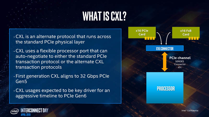
SK Hynix Licenses DBI Ultra 3D Interconnect Technology

Xperi Corporation today announced that it entered into a new patent and technology license agreement with SK hynix, one of the world's largest semiconductor manufacturers. The agreement includes access to Xperi's broad portfolio of semiconductor intellectual property (IP) and a technology transfer of Invensas DBI Ultra 3D interconnect technology focused on next-generation memory.

"We are delighted to announce the extension of our long-standing relationship with SK hynix, a world-renowned technology leader and manufacturer of memory solutions," said Craig Mitchell, President of Invensas, a wholly owned subsidiary of Xperi Corporation. "As the industry increasingly looks beyond conventional node scaling and turns toward hybrid bonding, Invensas stands as a pioneering leader that continues to deliver improved performance, power, and functionality, while also reducing the cost of semiconductors. We are proud to partner with SK hynix to further develop and commercialize our DBI Ultra technology and look forward to a wide range of memory solutions that leverage the benefits of this revolutionary technology platform."

Intel joins CHIPS Alliance to promote Advanced Interface Bus (AIB) as an open standard

CHIPS Alliance, the leading consortium advancing common and open hardware for interfaces, processors and systems, today announced industry leading chipmaker Intel as its newest member. Intel is contributing the Advanced Interface Bus (AIB) to CHIPS Alliance to foster broad adoption.

CHIPS Alliance is hosted by the Linux Foundation to foster a collaborative environment to accelerate the creation and deployment of open SoCs, peripherals and software tools for use in mobile, computing, consumer electronics and Internet of Things (IoT) applications. The CHIPS Alliance project develops high-quality open source Register Transfer Level (RTL) code and software development tools relevant to the design of open source CPUs, SoCs, and complex peripherals for Field Programmable Gate Arrays (FPGAs) and custom silicon.

Intel Unveils New Tools in Its Advanced Chip Packaging Toolbox

What's New: This week at SEMICON West in San Francisco, Intel engineering leaders provided an update on Intel's advanced packaging capabilities and unveiled new building blocks, including innovative uses of EMIB and Foveros together and a new Omni-Directional Interconnect (ODI) technology. When combined with Intel's world-class process technologies, new packaging capabilities will unlock customer innovations and deliver the computing systems of tomorrow.

"Our vision is to develop leadership technology to connect chips and chiplets in a package to match the functionality of a monolithic system-on-chip. A heterogeneous approach gives our chip architects unprecedented flexibility to mix and match IP blocks and process technologies with various memory and I/O elements in new device form factors. Intel's vertically integrated structure provides an advantage in the era of heterogeneous integration, giving us an unmatched ability to co-optimize architecture, process and packaging to deliver leadership products." -Babak Sabi, Intel corporate vice president, Assembly and Test Technology Development.

Toshiba Memory America Charts Course for PCIe 4.0 SSDs

Toshiba Memory America, Inc. (TMA), the U.S.-based subsidiary of Toshiba Memory Corporation, participated in the PCI-SIG (Peripheral Component Interconnect Special Interest Group) Compliance Workshop #109 in Burlingame, California, where several prototype and engineering samples of the company's upcoming PCIe 4.0 NVMe SSDs underwent PCI-SIG FYI Gen 4 testing.

The fourth generation of the PCIe interface, PCIe 4.0, doubles available bandwidth for graphics cards, SSDs, Wi-Fi, and Ethernet cards. The new standard will enable SSDs in particular to provide much higher performance than previous PCIe 3.0 SSDs, especially sequential read performance. An early participant seeking to enable PCIe 4.0 technologies, Toshiba Memory leverages its technology leadership role and actively collaborates with PCI-SIG and other member companies to accelerate adoption of the new interface standard.

"We realized years ago that the future of flash storage would be built on the NVMe architecture," noted John Geldman, director, SSD Industry Standards for Toshiba Memory America, Inc. and a member of the NVM Express Board of Directors. "This new and faster PCIe standard will maximize performance capability - unlocking systems' full potential."

Intel "Sapphire Rapids" Brings PCIe Gen 5 and DDR5 to the Data-Center

As if the mother of all ironies, prior to its effective death-sentence dealt by the U.S. Department of Commerce, Huawei's server business developed an ambitious product roadmap for its Fusion Server family, aligning with Intel's enterprise processor roadmap. It describes in great detail the key features of these processors, such as core-counts, platform, and I/O. The "Sapphire Rapids" processor will introduce the biggest I/O advancements in close to a decade, when it releases sometime in 2021.

With an unannounced CPU core-count, the "Sapphire Rapids-SP" processor will introduce DDR5 memory support to the data-center, which aims to double bandwidth and memory capacity over the DDR4 generation. The processor features an 8-channel (512-bit wide) DDR5 memory interface. The second major I/O introduction is PCI-Express gen 5.0, which not only doubles bandwidth over gen 4.0 to 32 Gbps per lane, but also comes with a constellation of data-center-relevant features that Intel is pushing out in advance as part of the CXL Interconnect. CXL and PCIe gen 5 are practically identical.

Intel Reveals the "What" and "Why" of CXL Interconnect, its Answer to NVLink

CXL, short for Compute Express Link, is an ambitious new interconnect technology for removable high-bandwidth devices, such as GPU-based compute accelerators, in a data-center environment. It is designed to overcome many of the technical limitations of PCI-Express, the least of which is bandwidth. Intel sensed that its upcoming family of scalable compute accelerators under the Xe band need a specialized interconnect, which Intel wants to push as the next industry standard. The development of CXL is also triggered by compute accelerator majors NVIDIA and AMD already having similar interconnects of their own, NVLink and InfinityFabric, respectively. At a dedicated event dubbed "Interconnect Day 2019," Intel put out a technical presentation that spelled out the nuts and bolts of CXL.

Intel began by describing why the industry needs CXL, and why PCI-Express (PCIe) doesn't suit its use-case. For a client-segment device, PCIe is perfect, since client-segment machines don't have too many devices, too large memory, and the applications don't have a very large memory footprint or scale across multiple machines. PCIe fails big in the data-center, when dealing with multiple bandwidth-hungry devices and vast shared memory pools. Its biggest shortcoming is isolated memory pools for each device, and inefficient access mechanisms. Resource-sharing is almost impossible. Sharing operands and data between multiple devices, such as two GPU accelerators working on a problem, is very inefficient. And lastly, there's latency, lots of it. Latency is the biggest enemy of shared memory pools that span across multiple physical machines. CXL is designed to overcome many of these problems without discarding the best part about PCIe - the simplicity and adaptability of its physical layer.

AMD Ryzen 3000 "Zen 2" BIOS Analysis Reveals New Options for Overclocking & Tweaking

AMD will launch its 3rd generation Ryzen 3000 Socket AM4 desktop processors in 2019, with a product unveiling expected mid-year, likely on the sidelines of Computex 2019. AMD is keeping its promise of making these chips backwards compatible with existing Socket AM4 motherboards. To that effect, motherboard vendors such as ASUS and MSI began rolling out BIOS updates with AGESA-Combo 0.0.7.x microcode, which adds initial support for the platform to run and validate engineering samples of the upcoming "Zen 2" chips.

At CES 2019, AMD unveiled more technical details and a prototype of a 3rd generation Ryzen socket AM4 processor. The company confirmed that it will implement a multi-chip module (MCM) design even for their mainstream-desktop processor, in which it will use one or two 7 nm "Zen 2" CPU core chiplets, which talk to a 14 nm I/O controller die over Infinity Fabric. The two biggest components of the IO die are the PCI-Express root complex, and the all-important dual-channel DDR4 memory controller. We bring you never before reported details of this memory controller.

Intel Acquires NetSpeed Systems for Chip Design and Interconnect Fabric IP

Intel today announced the acquisition of NetSpeed Systems, a San Jose, California-based provider of system-on-chip (SoC) design tools and interconnect fabric intellectual property (IP). Deal terms were not disclosed. NetSpeed's highly configurable and synthesizable offerings will help Intel more quickly and cost-effectively design, develop and test new SoCs with an ever-increasing set of IP. The NetSpeed team is joining Intel's Silicon Engineering Group (SEG) led by Jim Keller. NetSpeed co-founder and CEO, Sundari Mitra, will continue to lead her team as an Intel vice president reporting to Keller.
Intel is designing more products with more specialized features than ever before, which is incredibly exciting for Intel architects and for our customers. The challenge is synthesizing a broader set of IP blocks for optimal performance while reining in design time and cost. NetSpeed's proven network-on-chip technology addresses this challenge, and we're excited to now have their IP and expertise in-house.

Jim Keller, senior vice president and general manager of the Silicon Engineering Group at Intel

Intel to Acquire eASIC to Bolster FPGA Talent and Solutions

Intel is competing to win in the largest-ever addressable market for silicon, which is being driven by the explosion of data and the need to process, analyze, store and share it. This dynamic is fueling demand for computing solutions of all kinds. Of course Intel is known for world-class CPUs, but today we offer a broader range of custom computing solutions to help customers tackle all kinds of workloads - in the cloud, over the network and at the edge. In recent years, Intel has expanded its products and introduced breakthrough innovations in memory, modems, purpose-built ASICs, vision processing units and field programmable gate arrays (FPGAs).

FPGAs are experiencing expanding adoption due to their versatility and real-time performance. These devices can be programmed anytime - even after equipment has been shipped to customers. FPGAs contain a mixture of logic, memory and digital signal processing blocks that can implement any desired function with extremely high throughput and very low latency. This makes FPGAs ideal for many critical cloud and edge applications, and Intel's Programmable Solutions Group revenue has grown double digits as customers use FPGAs to accelerate artificial intelligence, among other applications.

Latest Intel Roadmap Slide Leaked, Next Core X is "Cascade Lake-X"

The latest version of Intel's desktop client-platform roadmap has been leaked to the web, which reveals timelines and names of the company's upcoming product lines. To begin with, it states that Intel will upgrade its Core X high-end desktop (HEDT) product line only in Q4-2018. The new Core X HEDT processors will be based on the "Cascade Lake-X" silicon. This is the first appearance of the "Cascade Lake" micro-architecture. Intel is probably looking to differentiate its Ringbus-based multi-core processors (eg: "Coffee Lake," "Kaby Lake") from ones that use Mesh Interconnect (eg: "Skylake-X"), so people don't compare the single-threaded / less-parallized application performance between the two blindly.

Next up, Intel is poised to launch its second wave of 6-core, 4-core, and 2-core "Coffee Lake" processors in Q1-2018, with no mentions of an 8-core mainstream-desktop processor joining the lineup any time in 2018. These processors will be accompanied by more 300-series chipsets, namely the H370 Express, B360 Express, and H310 Express. Q1-2018 also sees Intel update its low-power processor lineup, with the introduction of the new "Gemini Lake" silicon, with 4-core and 2-core SoCs under the Pentium Silver and Celeron brands.

PCI SIG Releases PCI-Express Gen 4.0 Specifications

The Peripheral Component Interconnect (PCI) special interest group (SIG) published the first official specification (version 1.0) of PCI-Express gen 4.0 bus. The specification's previous draft 0.9 was under technical review by members of the SIG. The new generation PCIe comes with double the bandwidth of PCI-Express gen 3.0, reduced latency, lane margining, and I/O virtualization capabilities. With the specification published, one can expect end-user products implementing it. PCI SIG has now turned its attention to the even newer PCI-Express gen 5.0 specification, which will be close to ready by mid-2019.

PCI-Express gen 4.0 comes with 16 GT/s bandwidth per-lane, per-direction, which is double that of gen 3.0. An M.2 NVMe drive implementing it, for example, will have 64 Gbps of interface bandwidth at its disposal. The SIG has also been steered toward lowering the latencies of the interconnect as HPC hardware designers are turning toward alternatives such as NVLink and InfinityFabric, not primarily for the bandwidth, but the lower latency. Lane margining is a new feature that allows hardware to maintain a uniform physical layer signal clarity across multiple PCIe devices connected to a common root complex. This is particularly important when you have multiple pieces of mission-critical hardware (such as RAID HBAs or HPC accelerators), and require uniform performance across them. The new specification also adds new I/O virtualization features that should prove useful in HPC and cloud computing.

Intel Announces New Mesh Interconnect For Xeon Scalable, Skylake-X Processors

Intel's "Xeon Scalable" lineup is designed to compete directly with AMD's Naples platform. Naples, a core-laden, high performance server platform that relies deeply on linking multiple core complexes together via AMD's own HyperTransport derived Infinity Fabric Interconnect has given intel some challenges in terms of how to structure its own high-core count family of devices. This has led to a new mesh-based interconnect technology from Intel.

Tech Industry Leaders Unite, Unveil New High-Perf Server Interconnect Technology

On the heels of the recent Gen-Z interconnect announcement, an aggregate of some of the most recognizable names in the tech industry have once again banded together. This time, it's an effort towards the implementation of a fast, coherent and widely compatible interconnect technology that will pave the way towards tighter integration of ever-more heterogeneous systems.

Technology leaders AMD, Dell EMC, Google, Hewlett Packard Enterprise, IBM, Mellanox Technologies, Micron, NVIDIA and Xilinx announced the new open standard to appropriate fanfare, considering the promises of an up-to 10x performance uplift in datacenter server environments, thus accelerating big-data, machine learning, analytics, and other emerging workloads. The interconnect promises to provide a high-speed pathway towards tighter integration between different types of technology currently making up the heterogeneous server computing's needs, ranging through fixed-purpose accelerators, current and future system memory subsistems, and coherent storage and network controllers.
Return to Keyword Browsing
May 21st, 2024 10:38 EDT change timezone

New Forum Posts

Popular Reviews

Controversial News Posts