News Posts matching #Moore's Law

Return to Keyword Browsing

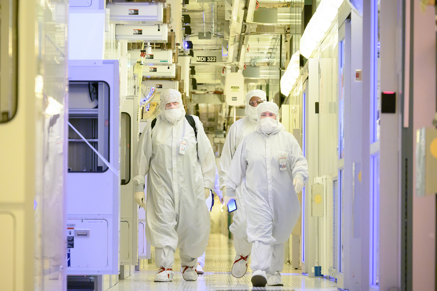
Intel Opens Fab 9 Foundry in New Mexico

Today, Intel celebrated the opening of Fab 9, its cutting-edge factory in Rio Rancho, New Mexico. The milestone is part of Intel's previously announced $3.5 billion investment to equip its New Mexico operations for the manufacturing of advanced semiconductor packaging technologies, including Intel's breakthrough 3D packaging technology, Foveros, which offers flexible options for combining multiple chips that are optimized for power, performance and cost.

"Today, we celebrate the opening of Intel's first high-volume semiconductor operations and the only U.S. factory producing the world's most advanced packaging solutions at scale. This cutting-edge technology sets Intel apart and gives our customers real advantages in performance, form factor and flexibility in design applications, all within a resilient supply chain. Congratulations to the New Mexico team, the entire Intel family, our suppliers, and contractor partners who collaborate and relentlessly push the boundaries of packaging innovation," said Keyvan Esfarjani, Intel executive vice president and chief global operations officer.

NVIDIA Chief Scientist Reaffirms Huang's Law

In a talk, now available online, NVIDIA Chief Scientist Bill Dally describes a tectonic shift in how computer performance gets delivered in a post-Moore's law era. Each new processor requires ingenuity and effort inventing and validating fresh ingredients, he said in a recent keynote address at Hot Chips, an annual gathering of chip and systems engineers. That's radically different from a generation ago, when engineers essentially relied on the physics of ever smaller, faster chips.

The team of more than 300 that Dally leads at NVIDIA Research helped deliver a whopping 1,000x improvement in single GPU performance on AI inference over the past decade (see chart below). It's an astounding increase that IEEE Spectrum was the first to dub "Huang's Law" after NVIDIA founder and CEO Jensen Huang. The label was later popularized by a column in the Wall Street Journal.

AMD Zen 5 Microarchitecture Referenced in Leaked Slides

A couple of slides from AMD's internal presentation were leaked to the web by Moore's Law is Dead, referencing what's allegedly the next-generation "Zen 5" microarchitecture. Internally, the performance variant of the "Zen 5" core is referred to as "Nirvana," and the CCD chiplet (CPU core die) based on "Nirvana" cores, is codenamed "Eldora." These CCDs will make up either the company's Ryzen "Granite Ridge" desktop processors, or EPYC "Turin" server processors. The cores themselves could also be part of the company's next-generation mobile processors, as part of heterogenous CCXs (CPU core complex), next to "Zen 5c" low-power cores.

In broad strokes, AMD describes "Zen 5" as introducing a 10% to 15% IPC increase over the current "Zen 4." The core will feature a larger 48 KB L1D cache, compared to the current 32 KB. As for the core itself, it features an 8-wide dispatch from the micro-op queue, compared to the 6-wide dispatch of "Zen 4." The integer execution stage gets 6 ALUs, compared to the current 4. The floating point unit gets FP-512 capabilities. Perhaps the biggest announcement is that AMD has increased the maximum cores per CCX from 8 to 16. At this point we don't know if it means that "Eldora" CCD will have 16 cores, or whether it means that the cloud-specific CCD with 16 "Zen 5c" cores will have 16 cores within a single CCX, rather than spread across two CCXs with smaller L3 caches. AMD is leveraging the TSMC 4 nm EUV node for "Eldora," the mobile processor based on "Zen 5" could be based on the more advanced TSMC 3 nm EUV node.

Intel Unveils Industry-Leading Glass Substrates to Meet Demand for More Powerful Compute

What's New: Intel today announced one of the industry's first glass substrates for next-generation advanced packaging, planned for the latter part of this decade. This breakthrough achievement will enable the continued scaling of transistors in a package and advance Moore's Law to deliver data-centric applications.

"After a decade of research, Intel has achieved industry-leading glass substrates for advanced packaging. We look forward to delivering these cutting-edge technologies that will benefit our key players and foundry customers for decades to come."
-Babak Sabi, Intel senior vice president and general manager of Assembly and Test Development

Intel to Develop Innovative Data Center Cooling Tech - Sponsored by US Energy Department

The U.S. Department of Energy (DOE) has announced its selection of Intel as one of 15 organizations tasked with developing high-performance, energy-efficient cooling solutions for future data centers. The award, announced in May, is part of the COOLERCHIPS program - Cooling Operations Optimized for Leaps in Energy, Reliability, and Carbon Hyperefficiency for Information Processing Systems - supported by DOE's Advanced Research Projects Agency-Energy (ARPA-E). Intel's project, anticipated to be a three-year agreement with $1.71 million in funding, will enable the continuation of Moore's Law by allowing Intel to add more cores and transistors to its highest performance processors, while managing the heat on future devices.

Tejas Shah, principal engineer and lead thermal architect for Intel's Super Compute Platforms Group said: "Immersion cooling is used for its simplicity, sustainability and ease of upgrades. This proposal will enable two-phase immersion cooling to align with the exponential increase in power expected by processors over the next decade."

AMD's Dr. Lisa Su Thinks That Moore's Law is Still Relevant - Innovation Will Keep Legacy Going

Barron's Magazine has been on a technology industry kick this week and published their interview with AMD CEO Dr. Lisa Su on May 3. The interviewer asks Su about her views on Moore's Law and it becomes apparent that she remains a believer of Gordon Moore's (more than half-century old) prediction - Moore, an Intel co-founder passed away in late March. Su explains that her company's engineers will need to innovate in order to carry on with that legacy: "I would certainly say I don't think Moore's Law is dead. I think Moore's Law has slowed down. We have to do different things to continue to get that performance and that energy efficiency. We've done chiplets - that's been one big step. We've now done 3-D packaging. We think there are a number of other innovations, as well." Expertise in other areas is also key in hitting technological goals: "Software and algorithms are also quite important. I think you need all of these pieces for us to continue this performance trajectory that we've all been on."

When asked about the challenges involved in advancing CPU designs within limitations, Su responds with: "Yes. The transistor costs and the amount of improvement you're getting from density and overall energy reduction is less from each generation. But we're still moving (forward) generation to generation. We're doing plenty of work in 3 nanometer today, and we're looking beyond that to 2 nm as well. But we'll continue to use chiplets and these type of constructions to try to get around some of the Moore's Law challenges." AMD and Intel continue to hold firm with Moore's Law, even though slightly younger upstarts disagree (see NVIDIA). Dr. Lisa Su's latest thoughts stay consistent with her colleague's past statements - AMD CTO Mark Papermaster reckoned that the theory is pertinent for another six to eight years, although it could be a costly endeavor for AMD - the company believes that it cannot double transistor density every 18 to 24 months without incurring extra expenses.
Return to Keyword Browsing
Apr 30th, 2024 18:40 EDT change timezone

New Forum Posts

Popular Reviews

Controversial News Posts