News Posts matching #Nehalem

Return to Keyword Browsing

Windows 11 24H2 Instruction Requirement Affects Older/Incompatible CPUs

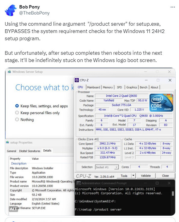
Systems running on older hardware could be excluded from upcoming public versions of Windows 11—the recently released preview/insider build (26052) has introduced all sorts of new features including "Sudo for Windows", an improved regedit, and hidden beneath the surface, an AI-flavored Super Resolution settings menu. Early partakers of version 24H2 are running into instruction set-related problems—Windows operating expert, Bob Pony, was one of the unlucky candidates. Microsoft's preview code seems to require a specific instruction set to reach operational status—Pony documented his frustrations on social media: "Using the command line argument "/product server" for setup.exe, BYPASSES the system requirement checks for the Windows 11 24H2 setup program. But unfortunately, after setup completes then reboots into the next stage. It'll be indefinitely stuck on the Windows logo boot screen."

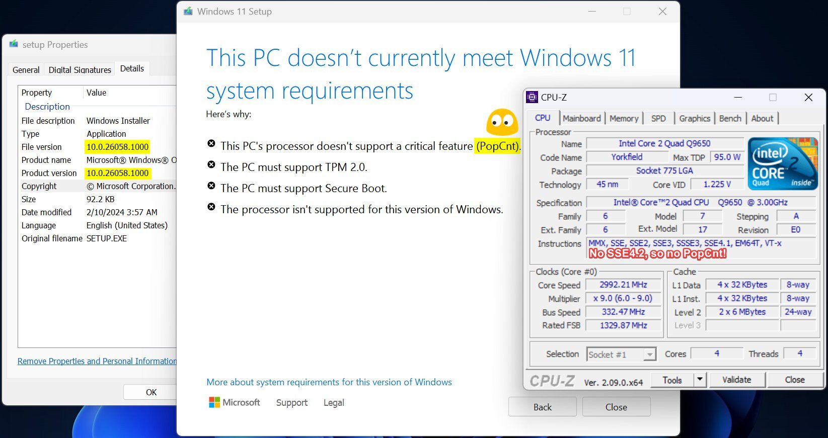
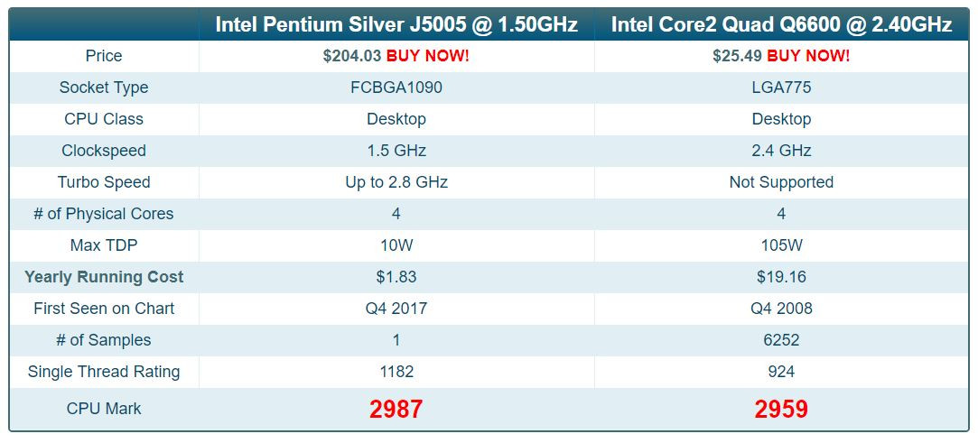
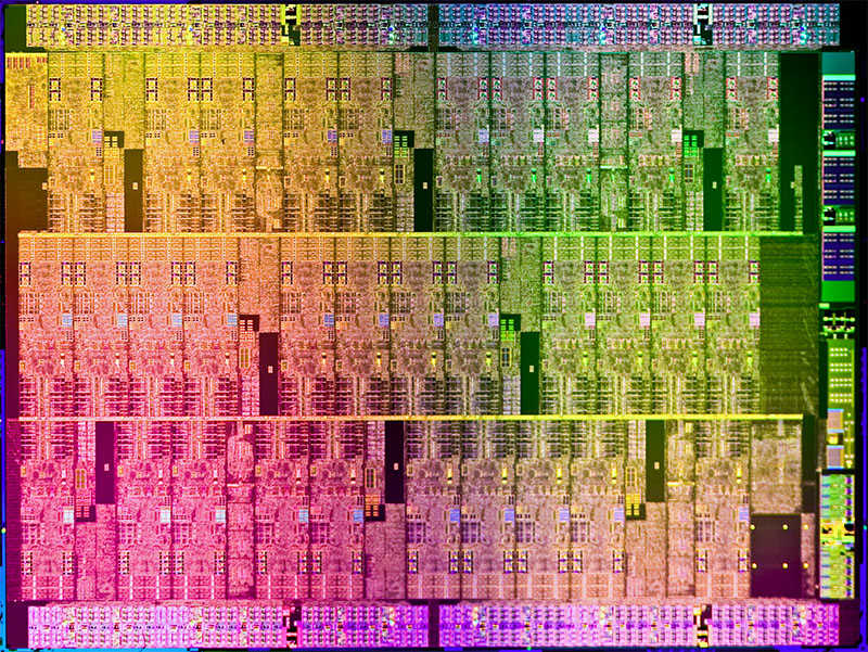
He continued to narrow in on the source of blame: "Windows 11 Version 24H2 Build 26058's setup (if ran in a live Windows Install) now checks for a CPU instruction: PopCnt." The Register provided some history/context on the SSE4 set: "POPCNT/PopCnt counts the number of bits in a machine word that have been set (or different from zero.) You might see it in cryptography and it has been lurking in CPU architectures for years, pre-dating Intel and AMD's implementation by decades." It is believed that Microsoft has deployed PopCnt as part of its push into AI-augmented software features, although a segment of online discussion proposes that an engineer has "accidentally enabled" newer CPU instruction sets. Tom's Hardware marked a line in the sand: "PopCnt has been supported since the Intel Nehalem and AMD Phenom II (microarchitecture) era—14 years ago—so compatibility won't be an issue for any modern systems. The only users that will be affected are enthusiasts running modified versions of Windows 11 on 15+ year-old chips like Core 2 Duos or Athlon 64." Bob Pony's long-serving Core 2 Quad Q9650 processor—a late summer 2008 product—was deemed unworthy by the preview build's setup process.

"Nehalem" Lead Architect Rejoins Intel to Work on New High-Performance Architecture

The original "Nehalem" CPU microarchitecture from 2008 was pivotal to Intel, as it laid the foundation for Intel's mainline server and client x86 processors for the following 12-odd years. Glenn Hinton, the lead architect behind "Nehalem," announced that he is rejoining Intel after 3 years of retirement, to work on a new high-performance CPU project. Hinton states that his decision to rejoin Intel out of his retirement was influenced by Pat Gelsinger joining the company as its new CEO. Jim Keller, a CPU architecture lead behind several commercially-successful architectures, recently left Intel after a brief stint leading an undisclosed CPU core project. Keller later took up the mantle of CEO at hardware start-up Tenstorrent.

Pat Gelsinger leading Intel is expected to have a big impact on its return to technological leadership in its core businesses, as highlighted in Gelsinger's recent comments on the need for Intel to be better than Apple (which he referred to as "that lifestyle company") at making CPUs, in reference to Apple's new M1 chip taking the ultraportable notebook industry by storm. The other front Intel faces stiff competition from, is AMD, which has achieved IPC parity with Intel, and is beating it on energy-efficiency, taking advantage of the 7 nm silicon fabrication process.

Intel Unveils a Clean-slate CPU Core Architecture Codenamed "Sunny Cove"

Intel today unveiled its first clean-slate CPU core micro-architecture since "Nehalem," codenamed "Sunny Cove." Over the past decade, the 9-odd generations of Core processors were based on incrementally refined descendants of "Nehalem," running all the way down to "Coffee Lake." Intel now wants a clean-slate core design, much like AMD "Zen" is a clean-slate compared to "Stars" or to a large extent even "Bulldozer." This allows Intel to introduce significant gains in IPC (single-thread performance) over the current generation. Intel's IPC growth curve over the past three micro-architectures has remained flat, and only grew single-digit percentages over the generations prior.

It's important to note here, that "Sunny Cove" is the codename for the core design. Intel's earlier codenaming was all-encompassing, covering not just cores, but also uncore, and entire dies. It's up to Intel's future chip-designers to design dies with many of these cores, a future-generation iGPU such as Gen11, and a next-generation uncore that probably integrates PCIe gen 4.0 and DDR5 memory. Intel details "Sunny Cove" as far as mentioning IPC gains, a new ISA (new instruction sets and hardware capabilities, including AVX-512), and improved scalability (ability to increase core-counts without running into latency problems).

Intel Demoes "Sunnycove" High Performance Core

Intel is inching closer to its December 12 "2018 Architecture Day" event targeted at assuring investors and channel partners that its short-term and intermediate-term CPU architecture roadmap looks competitive, by even demonstrating early prototypes of future architectures. One such exhibit revealed a processor demo platform codenamed "Sunnycove." It's not clear if this is a derivative of an upcoming CPU architecture (such as "Ice Lake,") or if it's the first fundamentally new CPU core design since "Nehalem."

The numbers put out by Intel scream "up to 75% more 7-zip performance," without elaborating whether they mean compression, decompression, or encryption. Speaking of the latter, this chip has some serious encryption chops, including support for new encryption instruction-sets that include SHA-NI (secure hash algorithm new instructions), and vector-AES. Much of the chip is designed to accelerate encryption, and its applications could be focused on the enterprise.

Custom BIOSes Harden Intel X58 Motherboards Against Meltdown and Spectre

Legendary soft-modder Regeneration released a vast collection of motherboard BIOS updates for socket LGA1366 motherboards based on Intel X58 Express chipset, because motherboard manufacturers have abandoned the 10-year old platform (yeah, it's been a decade since "Nehalem"!). The BIOSes have been made by transplanting the latest micro-code updates by Intel, which run all the way back to the 1st generation Core micro-architecture.

These are unofficial BIOSes which you use at your own risk, but they've been made by a person with more than two decades of fanfare in the PC enthusiast community, famous for unofficial, performance-enhancing NGO VGA drivers from his now defunct blog NGOHQ.com. Find the links to the BIOS of your X58 motherboard in this thread on TechPowerUp Forums (hosted externally).

Intel Pentium Silver J5005 Catches Up With Legendary Core 2 Quad Q6600

The Core 2 Quad Q6600 quad-core processor is close to many a PC enthusiast's heart. It was the most popular quad-core processor by Intel in the pre-Nehalem LGA775 era, and continues to be found to this date on builds such as home-servers. Over a decade later, Intel's low-power Pentium Silver J5005 quad-core processor, which enthusiasts won't consider for anything, appears to have caught up with the Q6600. A CPU Passmark submission by a Redditor compares the J5005 with the Q6600, in which the latter is finally beaten. The J5005 scored 2,987 marks, compared to the Q6600's 2,959 marks. It's interesting to note here, that the J5005 is clocked at just 1.50 GHz, compared to the 2.40 GHz of the Q6600. Its TDP is rated at just 10W, compared to 95-105W of the Q6600.

Ryzen Architect Jim Keller Joins Intel

Jim Keller, the VLSI guru who led the team behind AMD's spectacular comeback in the x86 processor market with "Zen," has reportedly quit his job at Tesla to join AMD's bête noire, Intel. Following his work on "Zen," Keller had joined Tesla to work on self-driving car hardware. Keller joins Raja Koduri at Intel, the other big former-AMD name, who led Radeon Technologies Group (RTG).

PC Perspective comments that big names like Keller and Koduri joining Intel could provide clues as to Intel's current state and the direction it's heading in. The company appears to be in a state of shake-up from a decade of complacency and lethargy in its core business. Koduri could be putting together a team of people familiar to him for a new clean-slate project. The last time Intel had a clean slate was ten years ago, with "Nehalem."

Intel Patches Remote Execution Flaw on Its CPUs - Active Since 2008

A bug in Intel's AMT (Active Management Technology), ISM (Standard Manageability) and SBT (Small Business Technology) firmware versions 6 to 11.6 sits unpatched since 2008 - a bug which allows "an unprivileged attacker to gain control of the manageability features provided by these products." Potentially, this could have led systems to be exploited for remote control and spyware infection (and maybe it did lead to that, and we just don't know about it.) Through this flaw, hackers could log into a vulnerable computer's hardware - outside the security features of the OS and any anti-virus suites - and silently install malware and other thriving pieces of malevolent coding. AMT having direct access to the computer's network hardware ensures this could have been done outside of local tampering. The vulnerable AMT service is part of Intel's vPro suite of processor features, so it's catering more to businesses and server boxes than for the usual consumer-based products - though we all know some hardware enthusiast's usage of this kind of processors in their personal rigs. If you don't have vPro or AMT present at all, you are in the clear. However, some outlets report that Intel systems are vulnerable to direct hardware access even if their AMT, ISM, or SBT implementations aren't provisioned - it's just the network access that doesn't work.

These insecure management features have been available in various Intel chipsets for nearly a decade, starting with the Nehalem Core i7 in 2008, all the way up to this year's Kaby Lake Core parts. Luckily, this "feature", which is present in millions of Intel chips and potentially provides a "backdoor-esque" entry point to equal millions of systems, appears to be able to be addressed through a microcode update. However, this update will have to be pushed by your system manufacturer, and you can probably begin to imagine by now how such a process will linger on, and how hard it will be for this to happen to every affected system.

Intel Plays Dirty Over Ryzen, Attempts to Manipulate Ryzen Reviews?

Intel is rattled with AMD Ryzen. Its 10-year old Nehalem CPU architecture that has been shrunk and incrementally updated over the years, is finally coming across as dated in the wake of AMD's "Zen" architecture. What to do when a competitor with 1/50th your R&D budget threatens to wreck your next annual appraisal? Play dirty and arm-twist the media of course! And playing dirty Intel is, according to a TweakTown report.

Apparently, Intel has scrambled its PR department to call in favors with the press in return for "guidelines" on how to review AMD Ryzen. Intel's PR emails allegedly ask reviewers to "call us before you write." The guidelines are worded more to make it sound like Intel wants its chips to be reviewed "fairly" against Ryzen, but the underlying objective is clear.

Moore's Law Buckles as Intel's Tick-Tock Cycle Slows Down

Intel co-founder Gordon Moore's claim that transistor counts in microprocessors can be doubled with 2 years, by means of miniaturizing silicon lithography is beginning to buckle. In its latest earnings release, CEO Brian Krzanich said that the company's recent product cycles marked a slowing down of its "tick-tock" product development from 2 years to close to 2.5 years. With the company approaching sub-10 nm scales, it's bound to stay that way.

To keep Moore's Law alive, Intel adopted a product development strategy it calls tick-tock. Think of it as a metronome that give rhythm to the company. Each "tock" marks the arrival of a new micro-architecture, and each "tick" marks its miniaturization to a smaller silicon fab process. Normally, each year is bound to see one of the two in alternation.

AMD to Emphasize on "Generation" with Future CPU Branding

AMD is planning to play a neat branding game with Intel. Branding of the company's 2016 lineup of CPUs and APUs will emphasize on "generation," much in the same way Intel does with its Core processor family. AMD will mention in its PIB product packaging, OEM specs sheets, and even its product logo (down to the case-badge), that its 2016 products (FX-series CPUs and A-series APUs) are the company's "6th generation." 2016 marks prevalence of Intel's Core "Skylake" processor family, which is its 6th generation Core family (succeeding Nehalem/Westmere, Sandy Bridge, Ivy Bridge, Haswell, and Broadwell). AMD is arriving at its "6th generation" moniker counting "Stars," "Bulldozer," "Piledriver," "Steamroller," and "Excavator," driving its past 5 generations of APUs, and the occasional FX CPU.

It turns out that the emphasis on "generation" is big with DIY and SI retail channels. Retailers we spoke with, say that they find it easier to break through Intel's often-confusing CPU socket change cycle, which ticks roughly every 18-24 months. Customers, they say, find it easier to simply mention the "generation" of Core processor they want, to get all relevant components to go with them (such as motherboard and memory bundles). While AMD's FX brand clearly didn't see generations beyond "Piledriver," the company's decision to unify the socket for its FX and A-Series product lines next year, with AM4, makes "6th generation FX processor" valid.

How Intel Plans to Transition Between DDR3 and DDR4 for the Mainstream

The transition between DDR2 and DDR3 system memory types was slower than the one between DDR and DDR2. DDR3 made its mainstream debut with Intel's X38 and P35 Express platforms, at a time when the memory controller was still within the domain of a motherboard chipset, at least in Intel's case. The P35 supported both DDR2 and DDR3 memory types, and motherboard manufacturers made high-end products based on each of the two memory types, with some even supporting both.

Higher module prices posed a real, and higher latencies, posed a less real set of drawbacks to the initial adoption of DDR3. Those, coupled with the limited system bus bandwidth, to take advantage of DDR3. DDR3 only really took off with Nehalem, Intel's first processor with an integrated memory controller (IMC). An IMC, again in Intel's case, meant that the CPU came with memory I/O pins, and could only support one memory type - DDR3. Since then, DDR3 proliferated to the mainstream. Will the story repeat itself during the transition between DDR3 and the new DDR4 memory introduced alongside Intel's Core i7 "Haswell-E" HEDT platform? Not exactly.

Intel Discontinues Xeon 5500 "Tylersburg" Platform

After last week's launch of the Xeon "Romley" platform, which replaces the Xeon 5500 "Tylersburg" platform, Intel has a retirement plan ready for the latter. Tylersburg was introduced in 2009, based on Intel's Nehalem architecture. Intel introduced product change notification (PCN) documents that detail these plans. The following models will be discontinued:
  • High-end: W5590, W5580, X5570, X5560 and X5550
  • Mid-tier versions: E5540, E5530, E5520, E5507, E5506, E5504, E5503 and E5502
  • Entry-level versions: L5530, L5520 and L5506
September 28, 2012 is set as the last date of orders for these chips. After this date, Intel will work to clear the last orders, and the products will attain end-of-life (EOL) status. Small stocks will still be held to honor any warranty claims.

Intel Aims at 10 nm Processors by 2018

It's not just host nations of the Olympics that are decided almost decades in advance, but also Intel's silicon names and the fab process they're going to be built on. Intel has its plan for the greater part of this decade already charted out, well beyond the upcoming Ivy Bridge architecture. Intel follows the "tick-tock" product cycle, where every micro-architecture gets to be built on two succeeding fab processes, and every fab process getting to have two succeeding micro-architectures built on it, in succession. Westmere is an optical shrink of the Nehalem architecture, it was a "tick" for the 32 nm process, Sandy Bridge is its "tock", and a new architecture. Ivy Bridge is essentially an optical shrink of Sandy Bridge, it is the "tick" for 22 nm process.

Ivy Bridge will make its entry through the LGA1155 platform in 2012, it will make up the 2012 Core processor family. Haswell is the next-generation architecture that succeeds Sandy Bridge and IvyBridge, it will be built on the 22 nm process, and is expected to arrive in 2013. Roswell is its optical shrink to 14 nm, slated for 2014. Looking deep into the decade, there's Skylake architecture, that will span across 14 nm and 10 nm processes with Skymont. This model ensures that Intel has to upgrade its fabs every 2 or so years, an entirely new micro-architecture every 2 or so years as well, while providing optical shrinks every alternating year. Optical shrinks introduce new features, increased caches, and allow higher clock speeds. 10 nm for processors by 2018 sounds realistic looking at the advancement of NAND flash technologies that are pushing the boundaries of fab process development. NAND flash is much less complex than processor development, and hence serve as good precursors to a new process.

2011 Intel Core Processor Pricing and Launch Dates Surface

Back in August, a report with details sourced from ComputerBase.de was bang-on in tabling what the 2011 Intel Core processor lineup is going to look like. With a little over a month to go for the market release of these processors, fresh details emerged that reveal pricing and precise availability dates of each model. To begin with, 9th January is D-day for the socket LGA1155 platform, when one can expect a large wave of motherboards to reach stores, along with 10 new Core i5, Core i7 "Sandy Bridge" quad-core processors.

The quad-core lineup consists of 7 Core i5 models. Based on a Sandy Bridge derivative silicon, these processors differ from the Core i7 models in having no HyperThreading (4 cores/4 threads), and 25% of the L3 cache being disabled (set at 6 MB). The lineup overall is seeing a clock speed increase compared to current-generation "Lynnfield" processors. The Core i5 lineup also includes an overclocker-friendly "K" model, which features an unlocked BClk multipler. The fastest in the lineup is the Core i7 2600/2600K, which is clocked at 3.40 GHz. With the default BClk (base clock) of Sandy Bridge running at 100 MHz (compared to 133 MHz on Nehalem/Westmere), one can expect very high multiplier values. It should also be easier to calculate speeds and keep track of, for overclockers.

NVIDIA Names Fermi Architecture Successors

At the GPU Technology Conference (GTC), an annual event hosted by NVIDIA, the company named the next two succeeding GPU architectures to Fermi (the current generation architecture on which are based GeForce 400 series GPUs). NVIDIA's next major GPU design change will come in the form of "Kepler", probably named after the German mathematician Johannes Kepler. The only concrete details about this architecture is that chips will be built on the 28 nanometer silicon fabrication process, and that going by the architecture's double-precision GPU compute performance per Watt represented on a graph, NVIDIA expects Kepler to be 4~5 times faster than Tesla, and over twice as fast as Fermi, again, at double-precision GPU compute performance per Watt.

Kepler is slated for 2011, though which part of the year will it be out (since AMD's answer to Fermi isn't far away), wasn't revealed. Looking much further away into the future, much like Intel mentioned Sandy Bridge's successor (Gesher) way back when unveiling Nehalem, NVIDIA talked about Kepler's successor slated for 2013. This one is called Maxwell, probably in honour of Scottish mathematician James Maxwell, with expectations of no less than three times the double-precision computation power per Watt of Kepler. These chips will be built on the 22 nanometer process.

Intel Unveils New Product Plans for High-Performance Computing

During the International Supercomputing Conference (ISC), Intel Corporation announced plans to deliver new products based on the Intel Many Integrated Core (MIC) architecture that will create platforms running at trillions of calculations per second, while also retaining the benefits of standard Intel processors.

Targeting high-performance computing segments such as exploration, scientific research and financial or climate simulation, the first product, codenamed "Knights Corner," will be made on Intel's 22-nanometer manufacturing (nm) process - using transistor structures as small as 22 billionths of a meter - and will use Moore's Law to scale to more than 50 Intel processing cores on a single chip. While the vast majority of workloads will still run best on award-winning Intel Xeon processors, Intel MIC architecture will help accelerate select highly parallel applications.

Intel to Introduce 8-core Xeon Nehalem-EX, 6-core Westmere-EP Processors This Month

Intel is set to introduce a series of eight-core Xeon server processors later this month, that are capable of running in four-socket servers. With HyperThreading technology enabled, each core can handle two threads, taking the logical CPU count on such servers up to 64. Each Nehalem-EX chip has 8 CPU cores with dedicated L2 caches of 256 KB, a shared L3 cache of 24 MB, and Turbo Boost technology that helps conserve power while also stepping up performance when needed. The die also features a memory controller with four DDR3 memory channels. Being based on the Nehalem architecture, the chips are built on the 45 nm HKMG process.

In related news, Intel will also introduce Westmere-EP processors later this month. These chips will be based on the 32 nm Westmere architecture, and are likely to have 6 cores, up to 12 logical CPUs per chip, 12 MB of L3 cache and three DDR3 memory channels. These chips will be suited for two-socket servers and workstations.

EVGA Names and Details its Dual-LGA1366 Enthusiast Motherboard

EVGA today named its dual-LGA1366 enthusiast-grade motherboard, so far known by the codename W555. After a short contest on the company's forums, the company came up with "EVGA Classified SR-2" for its name. SR stands for "super record" and 2 denoting the dual-socket design. The Classified SR-2 is a an entusiast-grade (read: overclocker friendly) implementation of the Tylersburg platform, supporting Intel socket LGA1366 processors with two QPI links (2P Xeon, etc.) As an addition, the board allows you to do something that's difficult on typical 2P server motherboards: it allows you to mix different models of Xeon processors, provided they're based on the same architecture, and series. For example, you can mix a Xeon 5520 with Xeon 5540. You can also mix a quad-core processor with a six-core processor, provided the quad-core part is based on the Westmere architecture (32 nm), not Nehalem (45 nm).

The board will also let you run a single 2P-capable processor in either sockets. DDR3 memory modules can be non-ECC or even ECC. 2P Xeon DRAM Multipliers / Uncore Multipliers are locked so you will only be able to use maximum 2:8 or 2:10 depending on segment of CPU. EVGA tells that the board supports 4-way SLI on its GTX 285 Classified VGA, but adds that a "future flagship GPU" also supports it. Could this be GeForce GTX 400 series having it as a standard feature? We have to wait and see. 4-way CrossFireX is supported.

Business PCs Arrive with New Intel Core vPro Processor Family

Intel Corporation today unveiled its 2010 Intel Core vPro processor family to meet the needs of businesses of all sizes for PCs with greater, more flexible performance, theft prevention and cost savings in a rapidly changing business computing environment. These and several other capabilities are at the heart of many new Intel-based business laptop and desktop computers beginning to roll out from computer manufacturers worldwide.

The Intel Core vPro processors arrive as business computing evolves with the emergence of video, Internet telephony, social networking and other heavyweight applications - in many cases running at the same time - making a computer's performance an even bigger priority.

Intel Unveils Core i5 6xx, 6x1 Series Dual-Core Processors

Intel today gave a go ahead for the media to publish reviews of its brand new dual-core processors under the Core i5 6xx and Core i5 6x1 series. The processors are based on the new "Clarkdale" processor die, and make use of the company's 32 nm next generation HKMG manufacturing process. Unlike conventional processor packages based on the Nehalem/Westmere architecture, the new processors move the northbridge component of the system onto the processor package, only that it is based on a separate 45 nm die within the package. The 32 nm processor die houses two processor cores along with up to 4 MB of L3 cache, while it is wired to a larger iGPU die which houses the dual-channel DDR3 memory controller, a graphics core, PCI-Express root complex, along with other components traditionally found on northbridge chips.

The first three models in the new Core i5 series are the 3.20 GHz Core i5 650, 3.33 GHz Core i5 660 and 661 (latter has a faster iGPU), and 3.46 GHz Core i5 670. These processors have the LGA-1156 package and are compatible with existing P55 Express chipset (albeit without the iGPU feature), along with the company's new H55 Express and H57 Express chipsets that support the Flexible Display Interface that provides connectivity to the processors' iGPUs. The new processors feature HyperThreading Technology, with which it provides the operating system with four logical CPUs (threads) to deal with, TurboBoost technology which powers down a core and overclocks the other when the task load is low. Pricing and availability will surface when the processors are formally announced, a little later this month. Meanwhile, motherboard manufacturers are ready with boatloads of new motherboard models based on Intel's two new chipsets. A compilation of links to major reviews on the internet can be found in the day's reviews list on the homepage.

EVGA Prepares High-end Dual-LGA1366 Motherboard

EVGA is keeping up its streak of releasing high-end motherboards for processors based on the new Intel Nehalem architecture, with a new dual-socket monstrosity. Slated for CES 2010, not much about this high-end workstation motherboard has been revealed beyond the picture below. From the looks of it, probably EVGA is making a high-end, overclocker-friendly dual LGA-1366 motherboard based on the Intel 5500 "Tylersburg" chipset with the usual ICH10R southbridge. Existing LGA-1366 processors that support dual-socket operation which includes Xeon 5500 series may work on it. Probably, a future high-end Intel Core family CPU is released that is capable of dual-socket setups, too. The picture reveals two LGA-1366 sockets, each powered by an 8-phase digital PWM circuit. Each socket is wired to six DDR3 DIMM slots supporting triple-channel memory for that socket. More this CES.

Transcend Ships 4GB aXeRam DDR3-2000 Memory Kits for Intel Core i5 Platforms

Transcend Information Inc., a worldwide leader in the manufacture of high-performance memory modules, today launched 4GB aXeRam DDR3-2000 memory kits for use with Intel's LGA1156 Core i5 and Core i7 platforms. The XMP-ready DDR3 kits are designed to operate at a blazing-fast clock frequency of 2000 MHz with an exceptionally low voltage of just 1.65V.

Featuring memory bandwidth up to an incredible 32GB/s, Transcend's new aXeRam dual-channel memory kit is rated at 2000MHz with timings of 9-9-9-24, allowing performance enthusiasts and gamers to take their Intel Core i5 platform to the next level of memory overclocking performance. The Core i5, based on Intel's new Nehalem architecture, is the first Intel processor to integrate both a 16-lane PCI Express 2.0 graphics port and a two-channel DDR3 memory controller, enabling all input/output and manageability functions to be handled by the single-chip Intel P55 core-logic.

Gulftown Product Name and Tentative Price Surfaces

Contrary to older reports, Intel will stick to the Core i7 brand identifier to sell its first consumer (client) six-core processor based on the Nehalem architecture, codenamed "Gulftown". The first offering of these socket LGA-1366 processors, is the Core i7 980X Extreme Edition. Its positioning and pricing shows that Intel will replace its current flagship desktop processor, the Core i7 975 Extreme Edition with it, and at the very same price-point of US $999 (in 1000 unit tray quantities).

A future price list also shows that the Core i7 980X Extreme Edition is slated for March 2010. A month ahead of its launch, Intel will introduce the Core i7 930, which succeeds the Core i7 920 at its price-point of $284. The Gulftown core will be manufactured on Intel's brand new 32 nm HKMG process, it features 6 processing cores with 12 threads (HyperThreading Technology), triple-channel DDR3 memory with its integrated memory controller, 6.4 GT/s QPI link to the Intel X58 Express chipset, 12 MB of L3 cache, compatibility to platforms that support the Core i7 9xx processors, and 130W TDP. The Core i7 980X Extreme Edition comes with a clock speed of 3.33 GHz, The Core i7 930 on the other hand, is a quad-core processor which runs at 2.80 GHz.

Intel Develops 'HPC-Optimized' 6-core Xeon Processors

Following AMD's recent success of its 6-core Opteron processor in the TOP500 supercomputer list, Intel has sensed a market for "HPC-optimized" processors, which the company expects will be out in the first half of 2010. These could be either variants of the Nehalem-EX multi-socket capable processors, or that by design, Nehalem-EX suits HPC (high-performance computing) applications better.

These 6-core processors will carry clock speeds higher than 8-core Xeon processors around that time. The processors will be able to work in systems with up to 256 processors (logical CPUs). In addition to these Intel also announced that it will be releasing a beta version of its Ct technology by the end of this year. Ct makes parallel programming in the C and C++ programming languages easier, by automatically optimizing code to exploit multi-core and many-core systems.
Return to Keyword Browsing
May 2nd, 2024 20:01 EDT change timezone

New Forum Posts

Popular Reviews

Controversial News Posts