News Posts matching #PCIe 5.0

Return to Keyword Browsing

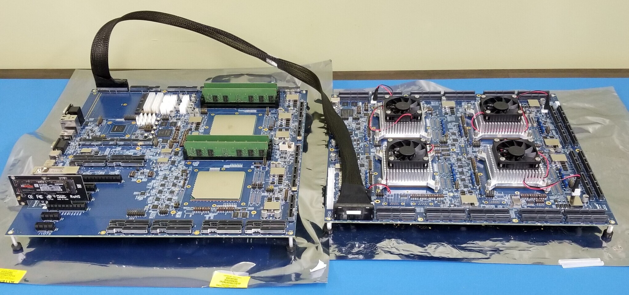
KIOXIA CD7 Series PCIe 5.0 SSDs Belt Out 14 GBps Sequential Transfers

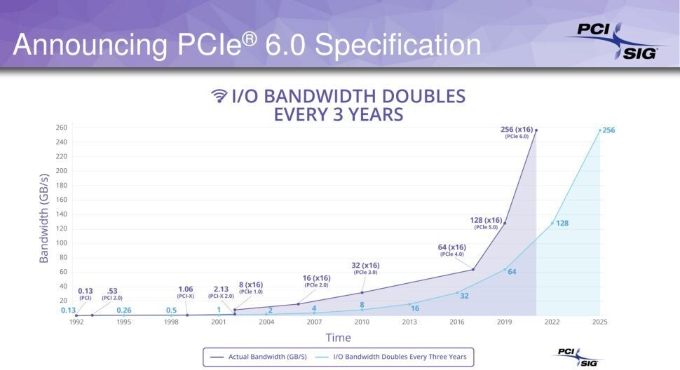
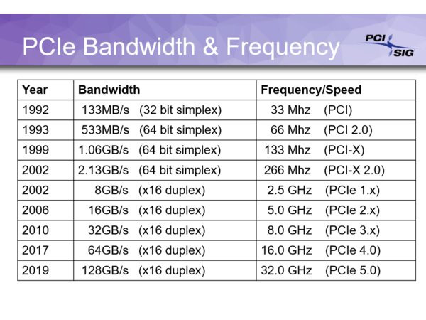
Presenting at the China Flash-Market Summit, KIOXIA unveiled its plans to leverage PCI-Express 5.0 to double SSD performance over the current generation. In typical 4-lane U.2 and M.2 connections, PCI-Express Gen 5 enables an interface bandwidth of 16 GB/s per direction (comparable to PCI-Express 3.0 x16). This means that accounting for interface overheads, typical PCIe Gen 5 SSDs will dance around the 11-15 GB/s (sequential) range. KIOXIA unveiled the CD7, a prototype enterprise SSD in the 2.5-inch EDSFF E3S form-factor with U.2 PCI-Express 5.0 x4 interface. This drive, the company claims, offers up to 14 GB/s sequential transfers, more than double the performance of the current CM6 series drives that leverage PCI-Express Gen 4.

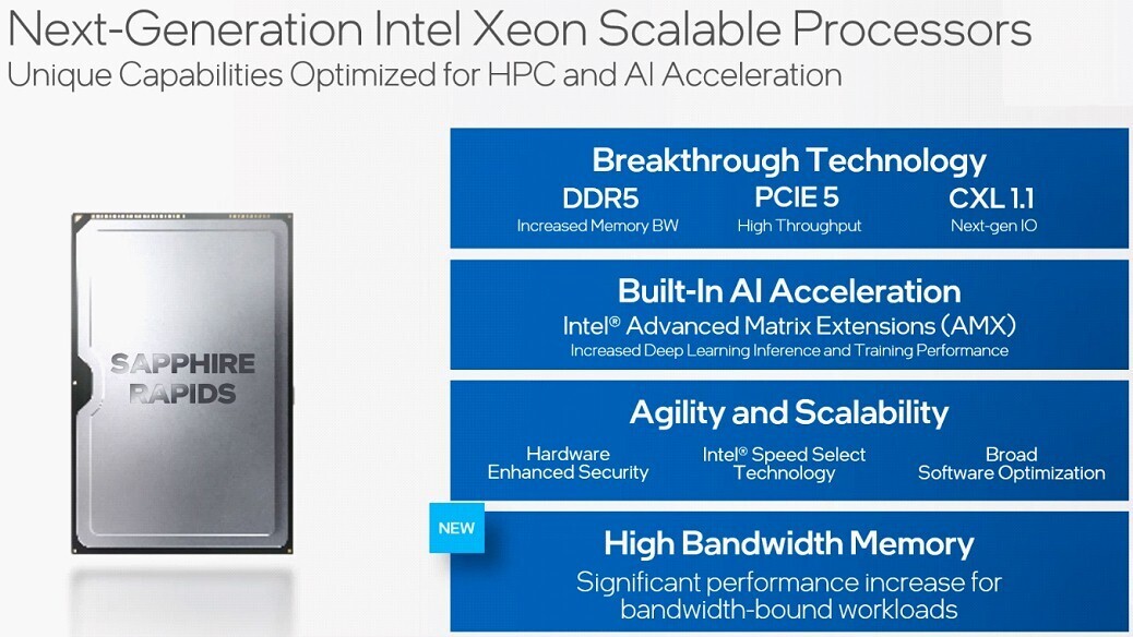
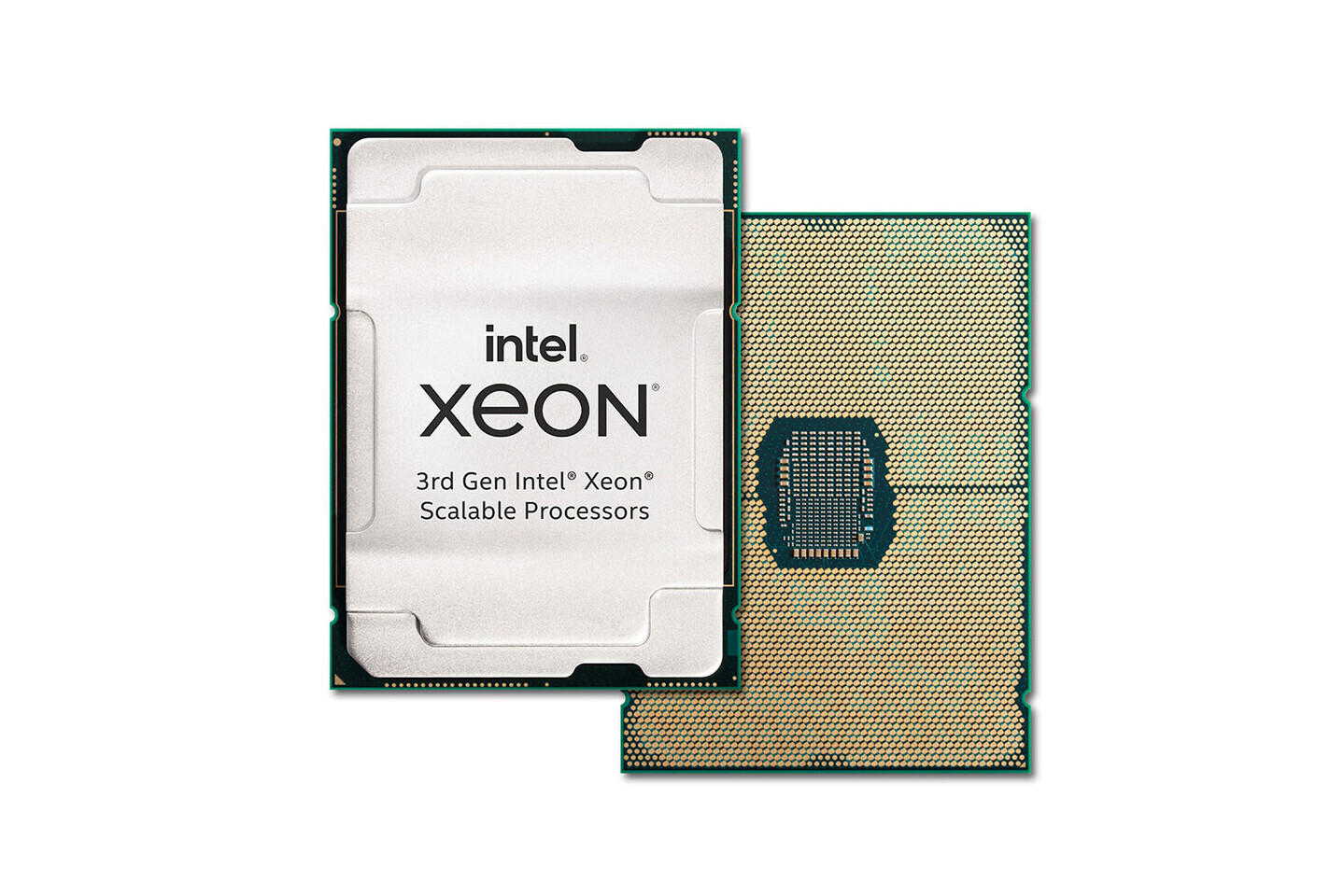
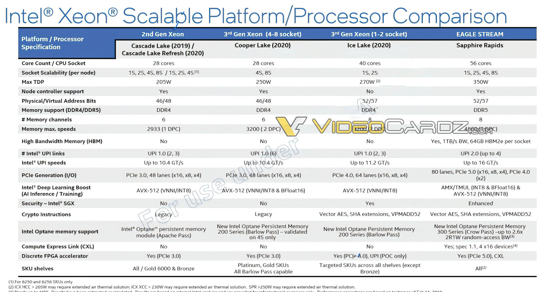
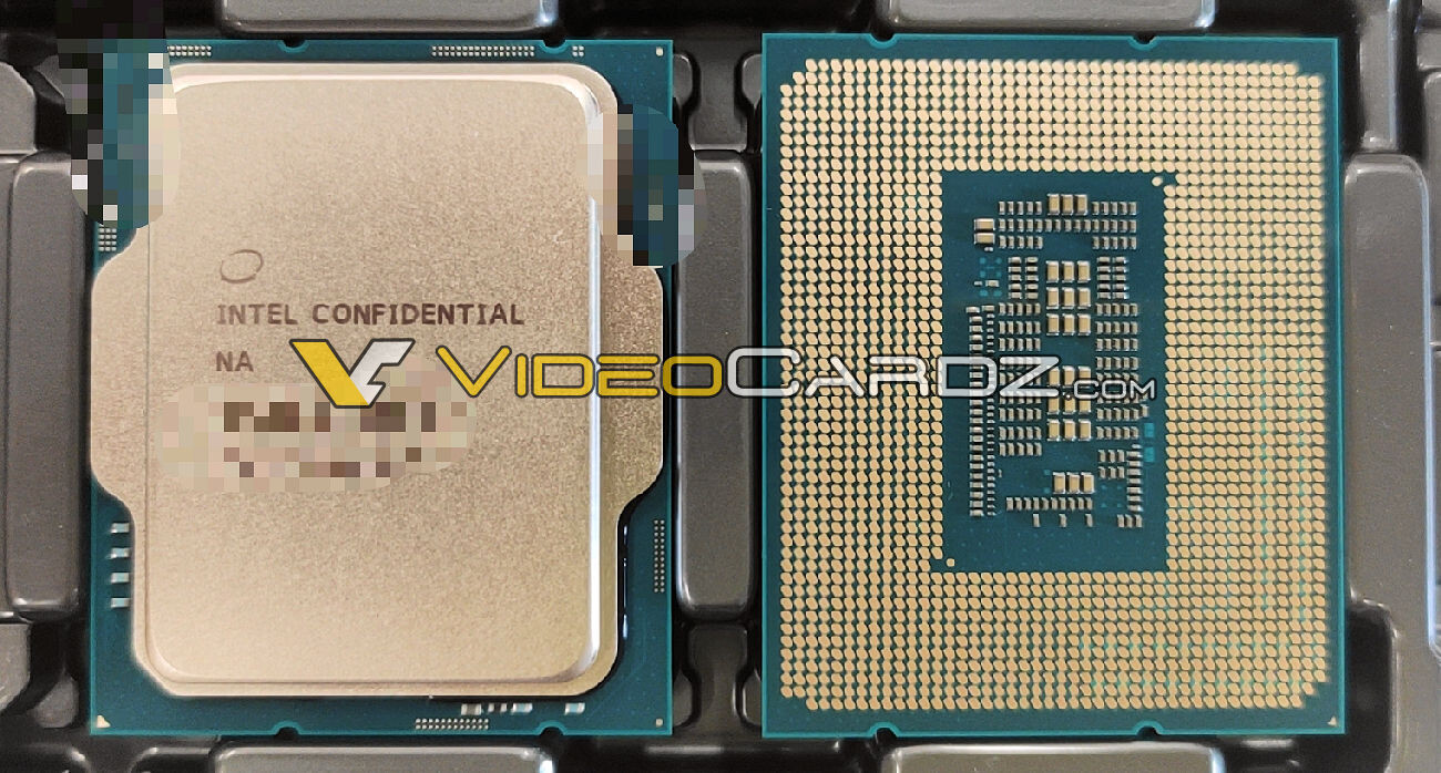
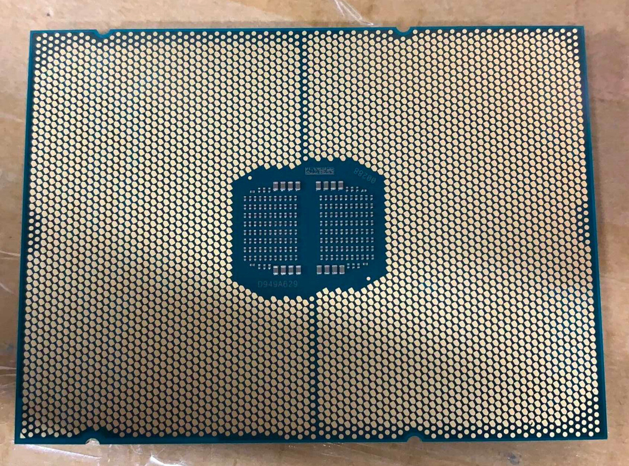
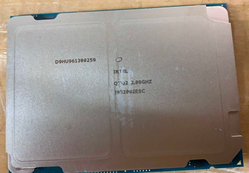
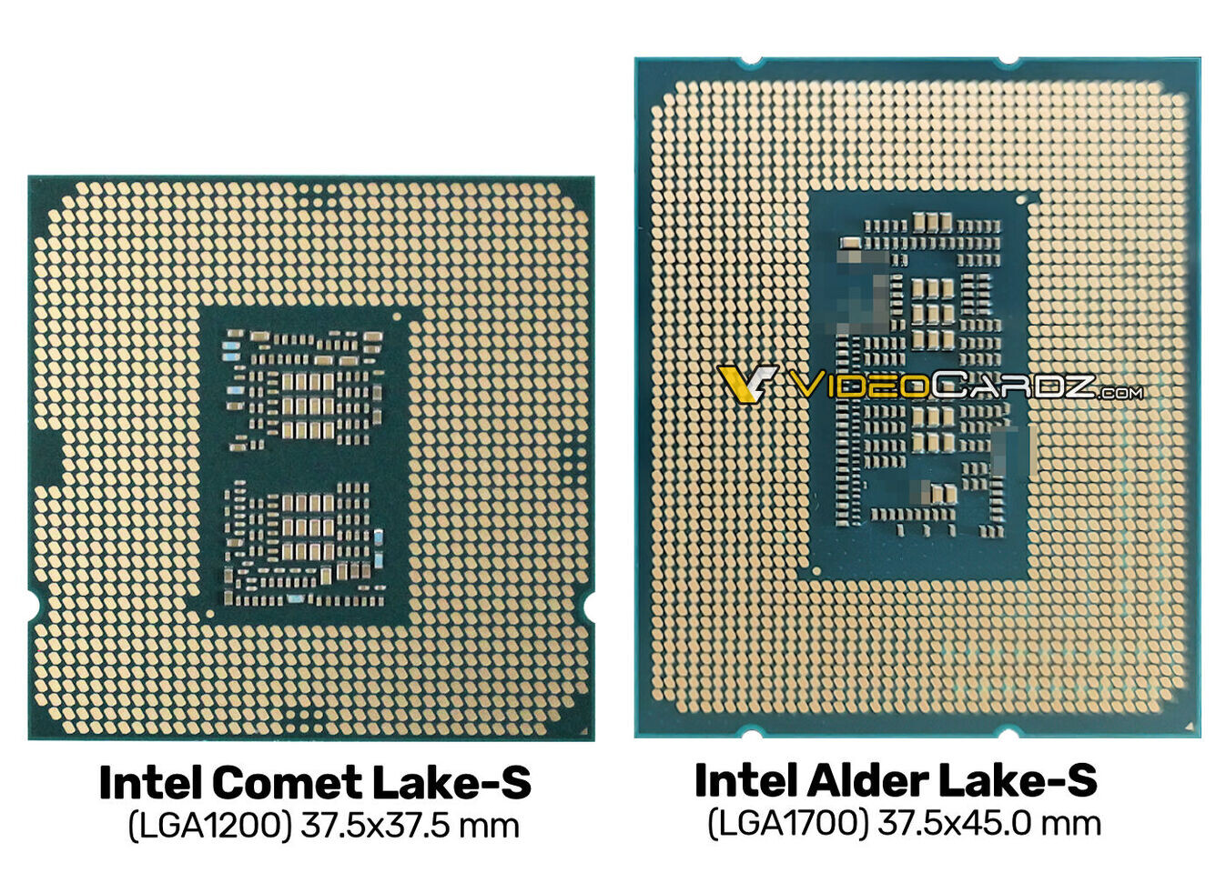
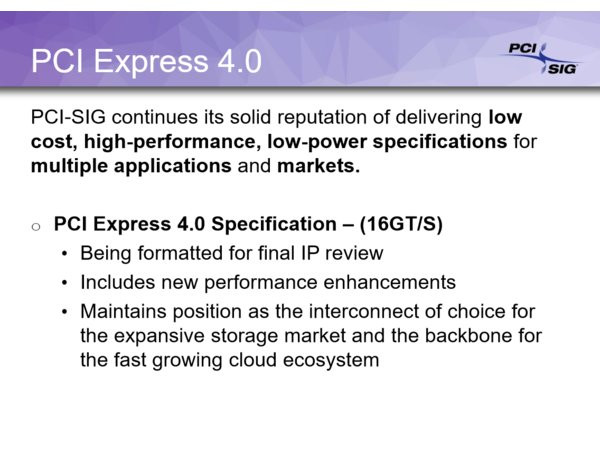
KIOXIA said that its first PCI-Express Gen 5 SSDs will begin shipping in Q4-2021, although it didn't mention if this was mass-market, or to select customers. The first enterprise platforms to leverage Gen 5 won't arrive before mid-2022, with Intel's Xeon "Sapphire Rapids" processors that feature PCI-Express Gen 5 support. KIOXIA sounded optimistic about the future growth in performance of SSDs. "Today, Moore's Law is technically dead in both the CPU and DRAM, but it still works at the PCIe clock rate," the company said, adding ""2015 [was] be the third generation of PCIe, 2019 is the fourth generation, and 2022 will be the fifth generation. Even if people spend a lot of money, they can't double CPU nodes to improve system performance, but buying Gen 5 SSD instead of Gen 4 SSD can greatly improve system performance."

Phison Enters High Speed IC Market with PCIe Gen 5.0 Components

Phison Electronics Corp., a global leader in NAND flash controller integrated circuits and storage solutions, today entered into the high-speed interface IC market with the introduction of its PS7101, a PCIe 5.0 Redriver IC with high gain and high linearity, which solves the signal attenuation caused by the transmission process on the motherboard or riser card in PCs and Servers.

Demand for the PCIe high-speed interface has significantly increased with the continuous development of semiconductor technology. PCIe 5.0 has quadrupled bandwidth over the previous standard in just a few years, with PCIe 6.0 expected to debut soon. Although the higher data rate of the chipset offers convenience to users, the development and design of the entire system has become increasingly more difficult. Specifically, the attenuation and the interference of noise in the motherboard eventually makes the signal between the CPU chip and the endpoints unable to be accurately transmitted and can even cause compatibility problems.

Intel Alder Lake-S to See Limited Launch of Enthusiast SKUs in 2021, Other Models Arrive 2022

Intel's 12th Generation Core "Alder Lake-S" desktop processor will see a limited launch in 2021, according to an Igor's Lab report. This will be restricted to PC enthusiast-relevant SKUs bearing the -K and -KF brand extensions, and compatible Socket LGA1700 motherboards based only on the top Z690 (Z590-successor) chipset. The series will ramp up to other (locked) models, along with more affordable chipset models (B560-successor), only by Q1-2022, on the sidelines of the 2022 International CES. Sources tell Igor's Lab that these select few models could be launched between October 25 and November 19.

Intel is expected to make several technological leaps over AMD with "Alder Lake-S." To begin with, it has the first hybrid core technology that combines high-performance "Golden Cove" cores with high-efficiency "Gracemont" cores, in a heterogenous multi-core setup comparable to Arm big.LITTLE. Next up, it is expected to debut the PCI-Express Gen 5 I/O, and DDR5 memory support. While PCIe 5.0 GPUs remain under development, the first devices to take advantage of it are expected to be NVMe SSDs, benefiting from 128 Gbps bandwidth (Gen 5 x4). It is also learned that the next-gen motherboards will retain the current ATX 24-pin + EPS power interface, and Intel won't force adoption of ATX12VO. The new ATX12VO standard increases motherboard costs as it essentially transfers DC-to-DC switching components from the PSU to the motherboard (12 V to 5 V; 12 V to 3.3 V, etc), and adds output connectors.

Intel Core i9-12900K Qualification Sample Reportedly Beats AMD Ryzen 9 5950X

The Intel Core i9-12900K is the companies upcoming flagship 12th Generation Alder Lake-S processor featuring a hybrid design with 8 high-performance cores and 8 high-efficiency cores. The qualification sample for the processor reportedly features a base clock of 3.9 GHz and a boost clock of 5.3 GHz which is less than initial rumors which claimed boost speeds could reach 5.5 GHz. The processor achieved a multi-core score of 11300 points in Cinebench R20 which is 800 points higher than AMD's flagship Ryzen 9 5950X. Intel's 12th Generation Alder Lake-S processors will be manufactured on the 10 nm Enhanced SuperFin node and will include support for PCIe 5.0 and DDR5. Intel is expected to announce the processors in Q3 2021 for a Q4 2021 release which will position them against AMD's upcoming V-Cache technology expected to arrive in early 2022.

Samsung Teases PCIe 5.0 Enterprise SSD Coming Q2 2022

Samsung has recently provided a few details of their PM1743 PCIe Gen 5 E3.S 1T EDSFF SSD set to release in Q2 2022. The PM1743 is an upcoming enterprise SSD from Samsung with PCIe 5.0 x4 connectivity which can enable a theoretical maximum speed of 15.7 GB/s. The SSD features V6 TLC NAND flash and comes with 1 Drive Writes Per Day (DWPD) of write endurance. The drive features an enterprise E3.S 1T single-width form factor (111.5 mm × 31.5 mm) popular in server deployments and will likely come with a TDP of 20-25 W. Samsung has provided a basic mechanical drawing of the SSD but we expect to find out more information closer to release.

Intel Xeon "Sapphire Rapids" Officially Shipping in Early 2022

Intel's Lisa Spelman, corporate vice president and general manager of the Xeon and Memory Group at Intel Corporation, has yesterday published a blog post talking about Intel's next-generation server platform codenamed Sapphire Rapids. The SPR platform is Intel's biggest step-up in the server processor space, and it is the exact CPU that will power the Aurora exascale supercomputer. Besides improvements to the CPU microarchitecture, the platform itself is bringing many benefits with it as well. It will use the latest industry protocols like DDR5 and PCIe 5.0. This is making a strong combination designed even for exascale supercomputers to be powered by this processor. However, the availability of this CPU was a bit of a mystery until yesterday. Below, you can see the quote from Ms. Lisa Spelman about the availability of said processors.
Lisa SpelmanDemand for Sapphire Rapids continues to grow as customers learn more about the benefits of the platform. Given the breadth of enhancements in Sapphire Rapids, we are incorporating additional validation time prior to the production release, which will streamline the deployment process for our customers and partners. Based on this, we now expect Sapphire Rapids to be in production in the first quarter of 2022, with ramp beginning in the second quarter of 2022.

Marvell Extends OCTEON Leadership with Industry's First 5nm DPUs

Marvell today introduced its new OCTEON 10 DPU designed to accelerate and process a broad spectrum of security, networking, and storage workloads required by demanding 5G, cloud, carrier and enterprise datacenter applications. With the increasing shift of workloads to the cloud, complex security requirements and the growing number of edge devices the demand for data centric compute has accelerated. By combining compute with best-in-class hardware accelerators, Marvell's OCTEON 10 DPU offers a significant TCO advantage and features numerous industry firsts. Delivering three times the performance and 50 percent lower power compared to previous generations of OCTEON, the newly announced solution is the first to be designed on a 5 nm process to incorporate Arm Neoverse N2 cores, as well as the first inline artificial intelligence/machine learning (AI/ML) hardware acceleration, the first integrated 1 terabit switch and the first to incorporate vector packet processing (VPP) hardware accelerators.

"To meet and exceed the growing data processing requirements for network, storage, and security workloads, Marvell focused on significant DPU innovations across compute, hardware accelerators, and high speed I/O," said John Sakamoto, vice president of Marvell's Infrastructure Processors Business Unit. "The OCTEON 10 brings compute leadership, supports networking and security workloads exceeding 400G, and incorporates leading edge I/O including DDR5 and PCIe 5.0."

Tachyum Receives Prodigy FPGA DDR-IO Motherboard to Create Full System Emulation

Tachyum Inc. today announced that it has taken delivery of an IO motherboard for its Prodigy Universal Processor hardware emulator from manufacturing. This provides the company with a complete system prototype integrating CPU, memory, PCI Express, networking and BMC management subsystems when connected to the previously announced field-programmable gate array (FPGA) emulation system board.

The Tachyum Prodigy FPGA DDR-IO Board connects to the Prodigy FPGA CPU Board to provide memory and IO connectivity for the FPGA-based CPU tiles. The fully functional Prodigy emulation system is now ready for further build out, including Linux boot and incorporation of additional test chips. It is available to customers to perform early testing and software development prior to a full four-socket reference design motherboard, which is expected to be available Q4 2021.

Samsung Preparing to Deploy 176-Layer V-NAND in PCIe 4.0, PCIe 5.0 SSD Products

Samsung is preparing to deploy their latest innovations in NAND density with the next-generation V-NAND (7th gen). Samsung says it is preparing products that leverage both V-NAND's higher density (at 176 layers per chip versus up to 136 layers on 6th gen) with the throughput of both PCIe 4.0 and PCIe 5.0. This would of course mean higher density drives available, as well as a reduction in the overall $/GB equation. Due to Samsung's vertical integration (meaning that they are one of the few companies that can design and produce all SSD components in-house), the company is also developing next-gen NAND controllers that can leverage throughputs of 2,000 MT/s transfer rates and thus "optimized for multitasking huge workloads".

Samsung expects to be able to scale V-NAND well past the 1,000 layer mark - a far-cry from the claims made by SK Hynix, who have only talked about a theoretical 600-layer NAND configuration. While the 176-layer, 7-gen V-NAND is only now entering mass production and the final stages of product development, Samsung has already taped out the initial batches of their 8th-gen V-NAND, which feature "more than 200 layers". It's likely that Samsung's 1,000-layer claim actually looks towards the future in a timeframe of decade(s?) and isn't actually something to look forward to in the approximate future.

Marvell Announces Bravera, World's First PCIe 5.0 SSD Controllers

Marvell today announced its new Bravera SC5 controller family, bringing unprecedented performance, best-in-class efficiency, and leading security features to address ever-expanding workloads in the cloud. The massive amount of data to be processed in cloud data centers is driving demand for faster and higher bandwidth storage in these environments. Marvell's Bravera SC5 SSD controllers address the critical requirements for scalable, containerized cloud storage infrastructure. By enabling the highest performing flash storage solutions, Marvell's controllers are poised to be the foundation for data centers that offer ultra-low latency, real-time applications while also providing cost-optimized, cloud-scale capacity.

As the industry's first SSD controllers to support PCIe 5.0 and NVMe 1.4b, Marvell's Bravera SC5 doubles the performance compared to PCIe 4.0 SSDs. This contributes to accelerated workloads and reduced latency, dramatically improving the user experience. In order to meet cloud service providers' stringent security requirements to ensure users' data is safe and protected, the controllers offer FIPS-compliant root of trust (RoT), AES 256-bit encryption and multi-key revocation. The new controllers are the first with a hardware-based Elastic SLA Enforcer to assure quality of service (QoS) and provide metering capabilities per customer to increase overall storage efficiency and utilization while lowering total cost of ownership (TCO).

Cadence Announces New Low-Power IP for PCI Express 5.0 Specification on TSMC N5 Process

Cadence Design Systems, Inc. (Nasdaq: CDNS) today announced immediate availability of Cadence IP supporting the PCI Express (PCIe ) 5.0 specification on TSMC N5 process technology. The next follow-on version on TSMC N3 process technology is expected to be taped out in early 2022. Collaboration with major customers is ongoing for N5 SoC designs targeting hyperscale computing and networking applications. The Cadence IP for PCIe 5.0 technology consists of a PHY, companion controller and Verification IP (VIP) targeted at SoC designs for very high-bandwidth hyperscale computing, networking and storage applications. With Cadence's PHY and Controller Subsystem for PCIe 5.0 architecture, customers can design extremely power-efficient SoCs with accelerated time to market.

The Cadence IP for PCIe 5.0 architecture offers a highly power-efficient implementation of the standard, with several evaluations from leading customers indicating it provides industry best-in-class power at the maximum data transfer rate of 32GT/s and worst-case insertion loss. Leveraging Cadence's existing N7/N6 silicon validated offering, the N5 design provides a full 512GT/s (gigatransfers per second) power-optimized solution across the full range of operating conditions with a single clock lane.

Intel's Upcoming Sapphire Rapids Server Processors to Feature up to 56 Cores with HBM Memory

Intel has just launched its Ice Lake-SP lineup of Xeon Scalable processors, featuring the new Sunny Cove CPU core design. Built on the 10 nm node, these processors represent Intel's first 10 nm shipping product designed for enterprise. However, there is another 10 nm product going to be released for enterprise users. Intel is already preparing the Sapphire Rapids generation of Xeon processors and today we get to see more details about it. Thanks to the anonymous tip that VideoCardz received, we have a bit more details like core count, memory configurations, and connectivity options. And Sapphire Rapids is shaping up to be a very competitive platform. Do note that the slide is a bit older, however, it contains useful information.

The lineup will top at 56 cores with 112 threads, where this processor will carry a TDP of 350 Watts, notably higher than its predecessors. Perhaps one of the most interesting notes from the slide is the department of memory. The new platform will make a debut of DDR5 standard and bring higher capacities with higher speeds. Along with the new protocol, the chiplet design of Sapphire Rapids will bring HBM2E memory to CPUs, with up to 64 GBs of it per socket/processor. The PCIe 5.0 standard will also be present with 80 lanes, accompanying four Intel UPI 2.0 links. Intel is also supposed to extend the x86_64 configuration here with AMX/TMUL extensions for better INT8 and BFloat16 processing.

Intel 12th Generation Alder Lake Platform Reportedly Brings 20% Single-Threaded Performance Uplift

Intel only just announced their 11th generation Rocket Lake-S desktop processors last week but we are already receiving information about the next generation Alder Lake-S platform which will finally make the jump to 10 nm. Intel slides for the upcoming family of processors have been leaked and they reveal some interesting information including a claimed 20% single-threaded performance increases from the new Golden Cove core design and 10 nm SuperFin node. The processors will feature Intel Hybrid Technology with a mix of small low-performance cores and large high-performance cores with a maximum of eight each for sixteen total cores. The processors will also include the latest connectivity with both PCIe 4.0 and PCIe 5.0 support along with DDR4 and DDR5 4800 MHz compatibility.

Intel will also be launching a new socket type called LGA1700 with a new package size which will render existing cooling solutions for LGA115X and LGA1200 sockets incompatible. The processors will also come with the launch of a new 600 Series chipset with PCIe 3.0 and PCIe 4.0 support along with the usual complement of USB, SATA, and networking. The entry-level 600-series motherboards will only support DDR4 memory at up to 3200 MHz while high-end Z690 motherboards will include DDR5 support. Intel has confirmed that they intend to launch Alder Lake later this year but it is yet to be known if they are referring to the desktop or mobile series.

Intel Rocket Lake-S Lands on March 15th, Alder Lake-S Uses Enhanced 10 nm SuperFin Process

In the latest round of rumors, we have today received some really interesting news regarding Intel's upcoming lineup of desktop processors. Thanks to HKEPC media, we have information about the launch date of Intel's Rocket Lake-S processor lineup and Alder Lake-S details. Starting with Rocket Lake, Intel did not unveil the exact availability date on these processors. However, thanks to HKEPC, we have information that Rocket Lake is landing in our hands on March 15th. With 500 series chipsets already launched, consumers are now waiting for the processors to arrive as well, so they can pair their new PCIe 4.0 NVMe SSDs with the latest processor generation.

When it comes to the next generation Alder Lake-S design, Intel is reported to use its enhanced 10 nm SuperFin process for the manufacturing of these processors. This would mean that the node is more efficient than the regular 10 nm SuperFin present on Tiger Lake processors, and some improvements like better frequencies are expected. Alder Lake is expected to make use of big.LITTLE core configuration, with small cores being Gracemont designs, and the big cores being Golden Cove designs. The magic of Golden Cove is expected to result in 20% IPC improvement over Willow Cove, which exists today in Tiger Lake designs. Paired with PCIe 5.0 and DDR5 technology, Alder Lake is looking like a compelling upgrade that is arriving in December of this year. Pictured below is the LGA1700 engineering sample of Alder Lake-S processor.

Silicon Motion: PCIe 5.0 SSD Controller to Arrive Next Year

With the debut of PCIe 4.0 standard, SSD manufacturers have started launching a new generation of storage devices, with unseen speeds before. Today's PCIe 4.0 SSDs can reach up to 8.0 GB/s reads and writes, all thanks to the bandwidth-heavy PCIe protocol. However, enterprise workloads are always requiring more and more bandwidth to satisfy their needs. Data is being moved in immense quantities and faster hardware is always welcome. The previous PCIe 4.0 standard is about to kneel to its successor - PCIe 5.0 protocol. Having double the amount of bandwidth, the new standard is set to bring unseen speeds.

The PCIe 5.0 protocol offers 32 GT/s per lane, making up to 64 GB/s in the full x16 implementation. However, when it comes to SSDs, as they use x4 lanes, it will increase the maximum speed to 16 GB/s, doubling the previous bandwidth. Silicon Motion, the maker of NAND flash controllers, has announced that the company is going to debut a PCIe 5.0 controller next year. "We are excited about enterprise-grade PCIe Gen5 controller, which we will have taped out early next year and sample in the second half of 2022", said Wallace Kuo, chief executive of Silicon Motion, during a conference call. Launching just in time to pair with Intel's Sapphire Rapids Xeon processors that support the PCIe 5.0 protocol, Silicon Motion is probably expecting to grab its market share there.

Microchip Announces World's First PCI Express 5.0 Switches

Applications such as data analytics, autonomous-driving and medical diagnostics are driving extraordinary demands for machine learning and hyperscale compute infrastructure. To meet these demands, Microchip Technology Inc. today announced the world's first PCI Express (PCIe) 5.0 switch solutions—the Switchtec PFX PCIe 5.0 family—doubling the interconnect performance for dense compute, high speed networking and NVM Express (NVMe ) storage. Together with the XpressConnect retimers, Microchip is the industry's only supplier of both PCIe Gen 5 switches and PCIe Gen 5 retimer products, delivering a complete portfolio of PCIe Gen 5 infrastructure solutions with proven interoperability.

"Accelerators, graphic processing units (GPUs), central processing units (CPUs) and high-speed network adapters continue to drive the need for higher performance PCIe infrastructure. Microchip's introduction of the world's first PCIe 5.0 switch doubles the PCIe Gen 4 interconnect link rates to 32 GT/s to support the most demanding next-generation machine learning platforms," said Andrew Dieckmann, associate vice president of marketing and applications engineering for Microchip's data center solutions business unit. "Coupled with our XpressConnect family of PCIe 5.0 and Compute Express Link (CXL ) 1.1/2.0 retimers, Microchip offers the industry's broadest portfolio of PCIe Gen 5 infrastructure solutions with the lowest latency and end-to-end interoperability."

Intel Confirms HBM is Supported on Sapphire Rapids Xeons

Intel has just released its "Architecture Instruction Set Extensions and Future Features Programming Reference" manual, which serves the purpose of providing the developers' information about Intel's upcoming hardware additions which developers can utilize later on. Today, thanks to the @InstLatX64 on Twitter we have information that Intel is bringing on-package High Bandwidth Memory (HBM) solution to its next-generation Sapphire Rapids Xeon processors. Specifically, there are two instructions mentioned: 0220H - HBM command/address parity error and 0221H - HBM data parity error. Both instructions are there to address data errors in HBM so the CPU operates with correct data.

The addition of HBM is just one of the many new technologies Sapphire Rapids brings. The platform is supposedly going to bring many new technologies like an eight-channel DDR5 memory controller enriched with Intel's Data Streaming Accelerator (DSA). To connect to all of the external accelerators, the platform uses PCIe 5.0 protocol paired with CXL 1.1 standard to enable cache coherency in the system. And as a reminder, this would not be the first time we see a server CPU use HBM. Fujitsu has developed an A64FX processor with 48 cores and HBM memory, and it is powering today's most powerful supercomputer - Fugaku. That is showing how much can a processor get improved by adding a faster memory on-board. We are waiting to see how Intel manages to play it out and what we end up seeing on the market when Sapphire Rapids is delivered.

Alleged Intel Sapphire Rapids Xeon Processor Image Leaks, Dual-Die Madness Showcased

Today, thanks to the ServeTheHome forum member "111alan", we have the first pictures of the alleged Intel Sapphire Rapids Xeon processor. Pictured is what appears to be a dual-die design similar to Cascade Lake-SP design with 56 cores and 112 threads that uses two dies. The Sapphire Rapids is a 10 nm SuperFin design that allegedly comes even in the dual-die configuration. To host this processor, the motherboard needs an LGA4677 socket with 4677 pins present. The new LGA socket, along with the new 10 nm Sapphire Rapids Xeon processors are set for delivery in 2021 when Intel is expected to launch its new processors and their respective platforms.

The processor pictured is clearly a dual-die design, meaning that Intel used some of its Multi-Chip Package (MCM) technology that uses EMIB to interconnect the silicon using an active interposer. As a reminder, the new 10 nm Sapphire Rapids platform is supposed to bring many new features like a DDR5 memory controller paired with Intel's Data Streaming Accelerator (DSA); a brand new PCIe 5.0 standard protocol with a 32 GT/s data transfer rate, and a CXL 1.1 support for next-generation accelerators. The exact configuration of this processor is unknown, however, it is an engineering sample with a clock frequency of a modest 2.0 GHz.

PCIe 6.0 Specification Reaches Milestone, Remains on Track for a 2021 Release

PCI-SIG has recently confirmed that version 0.7 of the PCIe 6.0 Specification has been officially released to its members. The PCI-SIG organization has already ratified the PCIe 5.0 standard and plans to release the full PCIe 6.0 specification in 2021. PCIe 6.0 will bring the same doubling in data rates seen with previous generations of the standard including a 2x improvement over PCIe 5.0, 4x boost over PCIe 4.0, and an 8x increase in speeds over the common PCIe 3.0 standard.

The organization has been speeding up its timeline for new versions of the PCIe specification with PCIe 3.0 being released in 2010 followed by PCIe 4.0 in 2017, PCIe 5.0 in 2019, and with PCIe 6.0 expected in 2021. The PCIe 6.0 standard is designed to fulfill the needs of future devices in the PC and enterprise markets such as 800 Gb/s Ethernet cards. The earliest we can expect to see PCIe 6.0 devices in the PC market would be 2023 or 2024 depending on requirements.

Intel Alder Lake-S Processor Pictured

Intel has just recently announced its next-generation Rocket Lake-S processor specifications designed to bring improved performance and newer platform technologies like PCIe 4.0. However, we are yet to see the first 10 nm CPU for desktop users. Today, thanks to the sources over at VideoCardz, we have the first look at Intel's next-next-generation processor called Alder Lake. The Alder Lake-S is a platform that brings many of the "firsts" for Intel. It will be the first architecture being built on the company's 10 nm SuperFin architecture. Alongside the new node, the platform will transition to the next-generation of technologies. Rumored are the transitions to PCIe 5.0 and perhaps, most importantly - DDR5.

Another new approach will be Intel's adaptation of Arm's big.LITTLE heterogeneous core structure. The processor will feature a few of the "little" cores for light tasks, and fire up the "big" cores for heavy computing. All of that will require a new socket to house the processor, which is the LGA1700. You can see the new processor below, compared to LGA1200 CPU from the previous generation.

Intel Alder Lake-S CPU Has Been Pictured

Intel has been preparing the launch of its 10 nm processors for desktop users for some time now, and today we are getting the first pictures of the Alder Lake-S CPU backside. Featuring a package with a size of 37.5×45 mm, the Alder Lake CPU uses more of its area for a pin count increase. Going up from 1200 pins in the LGA1200 socket, the new Alder Lake-S CPU uses 1700 CPU pins, which slots in the LGA1700 socket. In the picture below, there is an engineering sample of the Alder Lake-S CPU, which we see for the first time. While there is no much information about the processor, we know that it will use Intel's 10 nm SuperFin design, paired with hybrid core technology. That means that there will be big (Golden Cove) and little (Gracemont) cores in the design. Other features such as PCIe 5.0 and DDR5 should be present as well. The new CPU generation and LGA1700 motherboards are scheduled to arrive in second half of 2021.

Europe Readies its First Prototype of Custom HPC Processor

European Processor Initiative (EPI) is a Europe's project to kickstart a homegrown development of custom processors tailored towards different usage models that the European Union might need. The first task of EPI is to create a custom processor for high-performance computing applications like machine learning, and the chip prototypes are already on their way. The EPI chairman of the board Jean-Marc Denis recently spoke to the Next Platform and confirmed some information regarding the processor design goals and the timeframe of launch.

Supposed to be manufactured on TSMC's 6 nm EUV (TSMC N6 EUV) technology, the EPI processor will tape-out at the end of 2020 or the beginning of 2021, and it is going to be heterogeneous. That means that on its 2.5D die, many different IPs will be present. The processor will use a custom ARM CPU, based on a "Zeus" iteration of Neoverese server core, meant for general-purpose computation tasks like running the OS. When it comes to the special-purpose chips, EPI will incorporate a chip named Titan - a RISC-V based processor that uses vector and tensor processing units to compute AI tasks. The Titan will use every new standard for AI processing, including FP32, FP64, INT8, and bfloat16. The system will use HBM memory allocated to the Titan processor, have DDR5 links for the CPU, and feature PCIe 5.0 for the inner connection.

PCI-SIG Achieves 32 GT/s with New PCI-Express 5.0 Specification

PCI-SIG today announced the release of PCI Express (PCIe ) 5.0 specification, reaching 32 GT/s transfer rates, while maintaining low power and backwards compatibility with previous technology generations. "New data-intensive applications are driving demand for unprecedented levels of performance," said Al Yanes, PCI-SIG Chairman and President. "Completing the PCIe 5.0 specification in 18 months is a major achievement, and it is due to the commitment of our members who worked diligently to evolve PCIe technology to meet the performance needs of the industry. The PCIe architecture will continue to stand as the de facto standard for high performance I/O for the foreseeable future."

"For 27 years, the PCI-SIG has continually delivered new versions of I/O standards that enable designers to accommodate the never-ending increases in bandwidth required for next generation systems, while preserving investments in prior generation interfaces and software," noted Nathan Brookwood, research fellow at Insight 64. "Over that period, peak bandwidth has increased from 133 MB/second (for the first 32-bit parallel version) to 32 GB/second (for the V4.0 by16 serial version), a 240X improvement. Wow! The new PCIe 5.0 standard doubles that again to 64 GB/second. Wow2. We have come to take this increased performance for granted, but in reality, it takes a coordinated effort across many members of the PCI-SIG to execute these transitions so seamlessly."

PCI-SIG: PCIe 4.0 in 2017, PCIe 5.0 in 2019

After years of continued innovation in PCIe's bandwidth, we've hit somewhat of a snag in recent times; after all, the PCIe 3.0 specification has been doing the rounds on our motherboards ever since 2010. PCI-SIG, the 750-member strong organization that's in charge of designing the specifications for the PCIe bus, attribute part of this delay to industry stagnation: PCIe 3.0 has simply been more than enough, bandwidth-wise, for many generations of hardware now. Only recently, with innovations in storage mediums and innovative memory solutions, such as NVMe SSDs and Intel's Optane, are we starting to hit the ceiling on what PCIe 3.0 offers. Add to that the increased workload and bandwidth requirements of the AI field, and the industry now seems to be eager for an upgrade, with some IP vendors even having put out PCIe 4.0-supporting controllers and PHYs into their next-generation products already - although at the incomplete 0.9 revision.
Return to Keyword Browsing
May 21st, 2024 21:50 EDT change timezone

New Forum Posts

Popular Reviews

Controversial News Posts