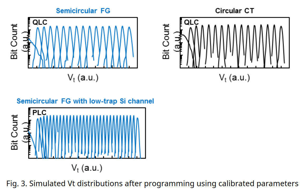
News Posts matching #QLC

Return to Keyword Browsing

Crucial Announces the P1 M.2 NVMe SSD with QLC NAND Flash

Crucial, a leading consumer brand of Micron Technology for memory and storage upgrades, today announced the availability of the Crucial P1 SSD, a PC storage device that leverages the NVMe PCIe interface and Micron's leading-edge QLC technology to deliver fast capacity for less. This is an expansion of Crucial's award-winning portfolio of dependable, high-performing, and affordable SSDs.

The Crucial P1 SSD delivers category-leading, real-world performance. PCMark 8 benchmarks show that the drive is capable of mixed-mode throughputs of up to 565 MB/s, with a composite score of 5,084, which outperforms similar SSDs within the price category. With sequential read/write speeds up to 2,000/1,700 MB/s, the P1 provides unwavering performance via hybrid-dynamic write acceleration, a unique SLC cache implementation. The drive offers an MTTF of 1.8 million hours and an endurance of up to 200 TB total bytes written, with power usage at an active average of 100mW.

3D QLC Woes - Manufacturers Fighting to Get Yields Above 50%

3D QLC (quad-level cell) is the latest, manufacture-ready technology to grace the NAND panorama, with promises of increased density over 3D TLC (triple-level cell), thus bringing pricing per GB even lower. However, as with all wafer-based PC components, yields are an extremely important part of that process. Cost reduction can only be attained if manufacturing allows for a given percentage of a wafer to be fully functional and without defects that compromise its feature-set or performance. However, as cell design becomes more complex in a bid to increase areal density, yields have taken longer to mature.

According to DigiTimes, 3D TLC yields have only gotten off the ground in the beginning of this year - right around the time companies were rolling out their 3D QLC designs. And if TLC took longer than expected to achieve respectable yields, it seems that QLC memory will take even longer - we already knew that the Intel-Micron venture on QLC was facing less than 50% yields, but DigiTimes has now extended this struggle to what seems to be the entire NAND manufacturing industry (Samsung Electronics, SK Hynix, Toshiba/ Western Digital and Micron Technology/Intel). The result? Expected price fluctuations in the beginning of 2019, as predicted production volume fails to meet both projected and actual demand, with 3D TLC supplies having to cope with increased market demands.

Intel-Micron QLC NAND Yields Less Than 50%, a Prelude to Global SSD Price Hikes?

IMFlash Technologies (IMFT), the Intel-Micron joint venture that manufactures NAND flash and 3D Xpoint memory for use in Intel and Micron end-user products, and Micron Technology-branded NAND flash supply to other SSD manufacturers, is facing a big hurdle with its QLC NAND flash manufacturing ramp-up, which if not checked, could influence SSD prices globally. The company is apparently seeing dangerously low yields of less than 50 percent for its 3D QLC NAND flash memory. This effectively makes its QLC NAND pricier (in terms of $/GB) than current-generation 3D TLC NAND.

The first victim of low yields of 3D QLC NAND flash is Intel's SSD 660p series, a mainstream NVMe SSD that brought 1 TB of storage under the $200-mark. Sources within IMFT tell Tweaktown that the company is seeing 48% yields in its 64-layer QLC NAND flash wafers (i.e. 52% of the wafer is unfit for further production). In contrast, 64-layer 3D TLC yields are above 90% (margin/incomplete dies are excluded from these figures). What's worse, the source predicts that the conditions may never get better with this generation.

Lite-On Unveils Powerful New SSD for Enterprise Workloads

At the Flash Memory Summit (FMS) 2018, LITE-ON Storage previewed the first EDSFF 1U solid-state drive (SSD) to emerge from its work with CNEX Labs. The revolutionary drive gained great interest among storage advocates.

In collaboration with such partners, LITE-ON delivers an innovative and highly efficient storage solution for scalable computing that aligns to Open Compute Project (OCP) specifications. The resulting EDSFF (Enterprise and Datacenter SSD Form Factor) SSD will provide a more cost-effective solution for enterprise and hyperscale cloud environments.

"Standard SSD solutions are great at handling many typical business workloads, but the complexity of storing information in both cloud and data center infrastructure requires SSD firmware to be flexible and adaptable," said Charlie Tseng, CEO of LITE-ON Storage. "LITE-ON's expertise in SSD firmware is perfect for the varying needs of customers."

NAND Flash Prices Could Reach $0.08/GB in 2019

Prices of NAND flash could drop to historic lows of $0.08 per gigabyte in 2019, according to Jim Handy from Objective Analysis, addressing delegates at the 2018 Flash Memory Summit. If you add the cost of the controller, optional DRAM chip, and other low-cost parts that make up an SSD, 480~512 GB drives under $70 could finally be a reality; followed by 1 TB under $120, and 2 TB under $200. Handy attributes the low prices to a catastrophic oversupply of NAND flash in the industry, which could push manufacturers to the brink of economic collapse.

The price drop is also accelerated with the introduction of the QLC (4 bits per cell) technology, which increases densities (and conversely decreases price/GB). Luckily, most NAND flash manufacturers also happen to make DRAM, and are offsetting some of their NAND flash losses with DRAM profits, as DRAM remains in undersupply. The NAND flash price-crash threatens to wipe out conventional hard-disk drives from the consumer-space, at least in matured markets; relegating them to developing markets.

SK Hynix Unveils 4D NAND Flash Memory Concept

3D NAND flash revolutionized flash storage as it used the third dimension (height) to stack multiple NAND flash layers, resulting in infinitesimally smaller footprint and reduced costs. SK Hynix believes that a "4-dimensional" NAND flash package is possible. Don't worry, such a stack doesn't look like a tesseract. Conventional 3D NAND flash relies on stacks of charge-trap flash (CTF) cells spatially located alongside its periphery block (which is responsible for wiring out each of the layers of the CTF stack). On a 2-D plane you'd be spending substrate real-estate on both the CTF and periphery block.

SK Hynix believes that the periphery block can be stacked along with the CTF stack, with microscopic vias wiring up the stack along the periphery, reducing the footprint of each cell stack. 4D stacking will also allow for greater number of CTF stacks per cell. Just to be clear, we're talking about stacks of cell and not stacks of NAND flash dies. The V5 cell-stack in SK Hynix's design entails 4 cells and periphery blocks sandwiched. The first implementation of this technology is a 96-layer 4D NAND flash chip with 512 Gb of capacity and TLC (3 bits per cell) density, although the technology is ready for QLC cells. This 512 Gb chip will begin sampling by the end of 2018, and the company is already working on a 1 Tb chip for 2019.

Intel Intros 660p Series M.2 NVMe SSDs with QLC NAND Flash

Intel Tuesday introduced the new SSD 660p series M.2 NVMe solid state drives. At the heart of these drives is the new 64-layer 3D QLC (quadruple level cell, or 4 bits per cell) NAND flash memory by IMFlash Technology (an Intel and Micron joint-venture). This memory is mated with a SIlicon Motion SMI 2263 controller. This chip is a derivative of the popular SMI2262EN, built on a newer process, with support for QLC NAND flash, compacted to have a smaller PCB footprint, and is driven by a custom firmware by Intel. The drives use over 10% of the QLC NAND flash area as SLC cache. The 660p series comes in three variants based on size - 512 GB, 1 TB, and 2 TB. The prices are the biggest dividend of QLC: the 512 GB variant goes for USD $99.99, the 1 TB variant at $199.99, and the 2 TB variant for $399.99.

Built in the M.2-2280 form-factor, the SSD 660p series drives feature PCI-Express 3.0 x4 interface. Intel's pricing puts these drives close to competing drives with PCIe x2 interface, but offering higher transfer rates thanks to the wider bus. It's also interesting to note here that the controller is cushioned by a DRAM cache (something PCIe x2 drives tend to lack, to keep costs down). Performance numbers differ by variant, and the 512 GB drive is the slowest, sequentially reading at speeds of up to 1500 MB/s, with up to 1000 MB/s sequential writes; up to 90,000 4K random reads, and up to 220,000 IOPS 4K random writes. The 1 TB and 2 TB variants both sequentially read and write at up to 1800 MB/s. The 1 TB variant offers 150,000 IOPS 4K random reads, and up to 220,000 IOPS random writes; while the 2 TB variant has 4K random reads/writes numbers of 220,000 IOPS.

Samsung starts Mass Production of QLC Consumer SSDs, 1 TB, 2 TB, 4 TB with over 520 MB/s Read/Write

Samsung Electronics, the world leader in advanced memory technology, today announced that it has begun mass producing the industry's first 4-bit (QLC, quad-level cell) 4-terabyte (TB) SATA solid-state drive (SSD) for consumers.

Based on 1-terabit (Tb) V-NAND with outstanding performance equivalent to the company's 3-bit design, Samsung's QLC SSD is expected to bring a new level of efficiency to consumer SSDs.

QLC NAND Flash Based Intel SSD 660p Could Lower Prices of PCIe x4 NVMe SSDs

Intel debuted its 3D QLC NAND flash memory on new SSD DC series 2.5-inch U.2 PCIe drives. Its technology partner Micron, too gave its 3D QLC an enterprise debut with the 5120 ION. The first client-segment debut from the IMFlash combine could be the Intel SSD 660p series of M.2 NVMe SSDs. Slotted between the 700p and the 600p, the new 660p implements homebrew 64-layer QLC NAND flash memory, and a new controller. It comes in sizes of 512 GB, 1 TB, and 2 TB.

The best part about the 660p is its performance numbers. The drive takes advantage of PCI-Express 3.0 x4, and offers (at least on paper), performance numbers identical to those of the pricier 700p. The drives read at speeds of up to 1800 MB/s, with up to 1100 MB/s writes. The 600p, in comparison, capped out at 560 MB/s sequential writes, while the 700p is only slightly higher, at 1200 MB/s. Random access speeds are up to 150,000 IOPS (both reads and writes). QLC pays off rich dividends to consumers by way of price/GB. The 660p 512 GB is expected to be priced at 113.90€ (0.22€/GB), the 1 TB variant at 197.75€ (0.20€/GB), and the 2 TB variant at 391.43€ (0.20€/GB). Not bad for launch prices, considering these are PCIe NVMe drives priced competitively with SATA SSDs.

Western Digital Releases 96-layer 3D QLC NAND with 1.33 Tb Capacity

Western Digital Corp. today announced successful development of its second-generation, four-bits-per-cell architecture for 3D NAND. Implemented for the company's 96-layer BiCS4 device, the QLC technology delivers the industry's highest 3D NAND storage capacity of 1.33 terabits (Tb) in a single chip. BiCS4 was developed at the joint venture flash manufacturing facility in Yokkaichi, Japan with our partner Toshiba Memory Corporation. It is sampling now and volume shipments are expected to commence this calendar year beginning with consumer products marketed under the SanDisk brand. The company expects to deploy BiCS4 in a wide variety of applications from retail to enterprise SSDs.

Intel Starts Producing 3D QLC NAND Flash Based PCIe SSDs for Data-Centers

Intel announced that it started mass-production of PCI-Express SSDs for data-centers that implement the latest-generation 3D QLC NAND flash memory. The new QLC (4 bits per cell) NAND flash memory enables 33% increases in densities over TLC NAND flash, and with 3D (stacks), the density per chip is further multiplied. Built in the 15 mm-thick 2.5-inch form-factor with U.2 interface, the drive is built for the rigors of "warm storage" (data that isn't hot, but isn't cold/archival, either). Such drives can be slower than "hot data" drives based on faster MLC or even SLC NAND flash, but almost always up; and faster than HDDs. The first 3D QLC NAND-based SSD, which probably uses the same chips as this drive, is the Micron 5210 ION, which was launched in May.

Toshiba Develops 96-layer BiCS FLASH with QLC Technology

Toshiba Memory Corporation, the world leader in memory solutions, today announced that it has developed a prototype sample of 96-layer BiCS FLASH, its proprietary 3D flash memory, with 4-bit-per-cell (quad level cell, QLC) technology that boosts single-chip memory capacity to the highest level yet achieved.Toshiba Memory will start to deliver samples to SSD and SSD controller manufacturers for evaluation from the beginning of September, and expects to start mass production in 2019.

The advantage of QLC technology is pushing the bit count for data per memory cell from three to four and significantly expanding capacity. The new product achieves the industry's maximum capacity of 1.33 terabits for a single chip which was jointly developed with Western Digital Corporation. This also realizes an unparalleled capacity of 2.66 terabytes with a 16-chip stacked architecture in one package. The huge volumes of data generated by mobile terminals and the like continue to increase with the spread of SNS and progress in IoT, and the need to analyze and utilize that data in real time is expected to increase dramatically. That will require even faster than HDD, larger capacity storage and QLC products using the 96-layer process will contribute a solution.

Samsung Electronics Brings Next Wave of High-Performance Storage with Mass Production of Fifth-Generation V-NAND

Samsung Electronics, the world leader in advanced memory technology, today announced that it has begun mass producing its fifth-generation V-NAND memory chips with the fastest data transfers now available. In the industry's first use of the 'Toggle DDR 4.0' interface, the speed for transmitting data between storage and memory over Samsung's new 256-gigabit (Gb) V-NAND has reached 1.4-gigabits per second (Gbps), a 40-percent increase from its 64-layer predecessor.

The energy efficiency of Samsung's new V-NAND remains comparable to that of the 64-layer chip, primarily because the operating voltage has been reduced from 1.8 volts to 1.2 volts. The new V-NAND also has the fastest data write speed to date at 500-microseconds (μs), which represents about a 30-percent improvement over the write speed of the previous generation, while the response time to read-signals has been significantly reduced to 50μs.

Realtek Intros RTS5762 NVMe SSD Controller Capable of 3500 MB/s Reads

Realtek, known more for its cheap Ethernet PHYs and audio CODECs, entered the SSD controller market in 2017, with mainstream SSD controllers. This year, the company plans to take on giants such as Silicon Motion, Phison, Intel, and Samsung, with its own high-performance controller, the RTS5762. The PCI-Express 3.0 x4 interface provides 4,000 MB/s of raw bandwidth per direction, and while it's technically impossible for any device to transfer its payload data at that speed (on account of various protocol overheads), very few PCI-Express 3.0 x4 SSDs get within 80th percentile of it (3200 MB/s per direction transfers). It's only recently that 3400 MB/s became the gold-standard of high-end M.2 NVMe SSDs, but Realtek plans to change that.

The RTS5762 is capable of up to 3,500 MB/s reads, or 87.5% saturation of the PCI-Experss 3.0 x4 bus. It supports up to 8 NAND flash channels, 3D TLC and 3D QLC NAND flash memory, and takes advantage of the newer NVMe 1.3 protocol. The only other controller right now that's capable of 3,500 MB/s reads is Samsung "Phoenix," found exclusively on the 970 Pro series (and no other brand's products). Sequential write performance is where this Realtek chip edges past Samsung, with the company showing CDM performance of up to 3,000 MB/s writes, whereas the 970 Pro is only specified to write up to 2,700 MB/s. Realtek also beefed up its mainstream NVMe controller portfolio with the new RTS5763DL. If drives based on this chip are priced right, it could carve out a new market segment between cheaper PCIe 3.0 x2 drives, and "upper mainstream" x4 drives such as the Samsung 970 EVO. Armed with just 4 NAND flash channels and no DRAM to cushion it, the RTS5763DL reads at up to 2150 MB/s, and writes at up to 1475 MB/s (as tested on CDM), making it faster than PCIe 3.0 x2 drives, at least in the sequential reads test.

Micron Ships Industry's First Quad-Level Cell NAND SSD

Micron Technology, Inc. has commenced shipments of the industry's first SSD built on revolutionary quad-level cell (QLC) NAND technology. Unveiled at Micron's 2018 Analyst and Investor Event, the Micron 5210 ION SSD provides 33 percent more bit density than triple-level cell (TLC) NAND, addressing segments previously serviced with hard disk drives (HDDs). The introduction of new QLC-based SSDs positions Micron as a leader in providing higher capacity at lower costs to address the read-intensive yet performance-sensitive cloud storage needs of AI, big data, business intelligence, content delivery and database systems.

As workloads evolve to meet the ever-increasing demands for real-time data insights and analytics, data centers increasingly need the capacity, speed, reliability and steady state performance that enterprise flash storage provides. Micron QLC NAND - reaching densities of 1 terabit with its next-generation 64-layer 3D NAND structure - is optimized to meet these demands and make SATA SSD performance and capacity more approachable than ever before.

Micron To Release QLC NAND-Based Drives in 2018 to the Server Environment

Micron has announced that they will be introducing QLC (Quad Level Cell) NAND-based, own brand drives for the server environment this year. The new QLC drives are expected to boost maximum storage density (and price per GB) closer to that of mechanical HDDs, which is why Micron is positioning drives based on this memory technology as data center-class SSDs for the nearline storage market. The company is positioning these drives as replacement options for 7,200 RPM HDDs for workloads that require heavy reads of stored information - thus offsetting QLC NAND's lower endurance when it comes to available maximum writes on the drives' cells.

It's a known trade-off when it comes to the NAND world: higher amounts of bits per cell to represent information means that there must be much increased accuracy when it comes to reading a given cell's voltage state. While SLC NAND only tracks two voltage states, MLC (2-bits per cell) tracks four voltage states, TLC doubles that to eight voltage states, and QLC doubles the ante again for a maximum 16 voltage states, where each voltage state represents data on the cell. Of course, with repeat writes and voltage changes, accuracy and capacity for the cell to maintain its given voltage tend to drop, which leads to incorrect information and thus corrupted data or those cells to be rendered inoperative. This is one of the reasons for manufacturers to include overprovisioning in their NAND-based solutions.

Marvell's Ready to launch QLC Controller Delivers 670K IOPS

QLC is the next big step in flash memory, with another bump in density increases and, crucially for consumers, revised, lower pricing for flash-based products that employ the new technology. We've already had a sneak peek at what QLC-based products can deliver - Intel's leaked SSD 660P employs QLC memory and is expected to deliver 1,800 MB/s in sequential read and up to 1,200 MB/s in sequential write speeds with 150,000 IOPS. Expect base drive capacities to increase - QLC being higher density would mean fewer NAND chips, but manufacturers want to keep the added performance of chip parallelism.

However, flash needs controllers to deliver its true potential, and Marvell has one up its sleeve. The new controller will eventually replace the NVMe 1.1 Eldora (88SS1093) used in some popular SSDs that are already shipping, such as Plextor's M9Pe, and the folks at Tom's hardware took a peek at it - running the current TLC memory, that is. The controller delivered over 670,000 IOPS and 3,500 MB/s in the demo, though there's no information on the density of the drive. But for those performance levels, it must've had a good amount of silicon. While not representative of final QLC memory performance of the controller, it's good to know that at least this part of the ecosystem is good to go. Now if only QLC was quick and hot off the presses, we could see a $100 512 GB SSD.

Intel SSD 760p and 660p Specifications and Pricing Listed Online

Autobuy, a popular online shopping site in Taiwan, recently listed Intel's upcoming 760p and 660p M.2 NVMe SSDs on their store. The SSD 760p will be manufactured under Intel's 64-layer 3D NAND technology and feature TLC (triple-level-cell) NAND. It's obviously the faster of the two with a sequential read speed up to 3,200 MB/s and a write speed up to 1,600 MB/s. The drive offers random access reads up to 350,000 IOPS and writes up to 280,000 IOPS. Intel will offer this model in capacities of 128 GB, 256 GB, 512 GB, 1 TB, and 2 TB. TigerDirect listed the pricing for them at $96, $120, $240, $448, and $893, respectively.

The SSD 660p is Intel's budget-friendly this time around. Therefore, it will use QLC (quad-level-cell) NAND despite being manufactured with the same technology as its older brother. This SSD can reach up to 1,800 MB/s in sequential read and up to 1,200 MB/s in sequential write speeds with random access read and write performance in the range of 150,000 IOPS. Surprisingly, Intel won't be offering this model in the 128 GB and 256 GB capacities. Instead, the lowest capacity model will start from 512 GB and make its way up to 2 TB. Unfortunately, pricing wasn't available at the time of this article.

Toshiba Unveils RC100 Series M.2 NVMe SSDs

Toshiba Memory America, Inc. (TMA), the U.S.-based subsidiary of Toshiba Memory Corporation, will be highlighting the use of its industry-leading BiCS FLASH 3D memory in several applications - including its new lineup of NVMe SSDs, the RC100 Series.

At CES, TMA is collaborating with its customers and technology partners to take on the future - together. Toshiba was the first company in the world[1] to announce 3D flash memory technology, which effectively addresses the processing, storage and management of the growing volume of data generated worldwide. Recent announcements see the company continuing to lead the industry forward, including the introduction of a 96-layer 512Gb die; the debut of the industry's first[2] flash memory device with quadruple-level cell (QLC) technology; and the addition of Through Silicon Via (TSV) technology. Already enabling the enterprise, data center, PC and mobile applications of today, TMA's BiCS FLASH has paved the way for the applications of tomorrow. In everything from artificial intelligence and virtual reality to a growing number of automotive applications (such as infotainment), high performance computing and the ever-expanding "internet of things," storage density needs will climb higher and higher - and BiCS FLASH was designed with this in mind.

Phison Also Looking to Introduce High performance E12 and S12 NAND Controllers

Phison isn't just a budget controller brand, as you well know, so in addition to their interesting, 2-channel NVMe NAND controller in the Phison E8, which should see products hitting retail in the following months, the company is also catering to the high performance crowds with the impressive E12 and S12 controllers. The E12 is definitely the star of Phison's new controller line-up - just look at those ratings of 3200 MB/s sequential read, 3000 MB/s sequential write, and 600K random read and random write IOPS. Naturally, those rated speeds should be taken with a measure of salt, as NAND type, its implementation and firmware tweaks all matter tremendously in extracting the best possible performance from high speed storage.

Contrary to the E8 budget Phison controller, the E12 will feature a full NVMe PCIe x4 interface, which allows for those speed ratings. The S12, on the other hand, is a more common SATA III controller, which means that its speeds of 550 MB/s sequential read and 530 MB/s sequential write are already hitting the interface's limits. Other than the interface and the rated speeds and IOPS, though, the specs are the same on these controllers: support for 3D NAND on MLC/TLC/QLC arrangements, 8-channel, LDPC, SmartECC, and End-to-End DPP support.

Samsung Readies 970 and 980 Series NVMe SSDs

At its Flash Memory Summit booth, Samsung revealed plans to launch new consumer-segment SSDs which succeed its current 960 EVO and 960 Pro series. Over 2017-18, the company is expected to launch the new 970 series and 980 series NVMe SSDs. Tom's Hardware predicts that Samsung could dispose of the "EVO" and "Pro" brand extensions to a static model number (such as 960 or 950). Samsung could tap into its current 3-bit per cell (TLC) 64-layer 3D V-NAND flash memory for the 970 and 980 series. With the company busy capacity-building for 4-bit per cell (QLC), the new SSD lines may not feature it, although Samsung is capable of surprising with aggressive launch cycles. As drives supporting the NVMe protocol, the 970 and 980 series could ship in modern form-factors, such as M.2 and U.2.

Toshiba's 768 Gb 3D QLC NAND Flash to Match TLC's Program/Erase Cycles

Not all news coming out of Toshiba is bad or somewhat bad. The Japanese giant still is one of the biggest players in the NAND semiconductor business, no matter the recent woes. Even more recently, though, Toshiba announced they had developed quadruple level cell NAND memory, which should improve density and, therefore, reduce the price/GB ratio on future consumer products, such as SSDs. However, each increase in the number of cell levels bring concerns regarding not only performance, but especially durability, since a higher number of states per cell increases the voltage steps that are applied to it (SLC NAND dealt with two voltage states, MLC with four, TLC with eight voltage states, and QLC will handle 16 of these.) This tends to make errors more common, and the cell's longevity to be compromised due to the amount of variation in its states, which means more powerful error correction techniques must be employed.
According to Toshiba, its 3D QLC NAND targets around ~1000 program/erase cycles, which is close to TLC NAND flash. This is considerably higher than the amount of P/E cycles (100 - 150) expected for QLC by the industry, which means the company has achieved what many thought difficult. Toshiba has begun sampling of its 3D QLC NAND memory devices earlier this month. everything points to mass production on late 2018, early 2019, though, which means we still have a long way to go until we see this technology implemented. This won't be the one to save us from escalating NAND prices; we'll have to look to other, more market and supply-and-demand based factors instead.

Toshiba Develops World's First 4-bit Per Cell QLC NAND Flash Memory

Toshiba America Electronic Components, Inc. (TAEC) today announced the latest generation of its BiCS FLASH three-dimensional (3D) flash memory. The newest BiCS FLASH device features 4-bit-per-cell, quadruple-level cell (QLC) technology and is the first 3D flash memory device to do so. Toshiba's QLC technology enables larger (768 gigabit) die capacity than the company's third-generation 512Gb 3-bit-per-cell, triple-level cell (TLC), and pushes the boundaries of flash memory technology.

Toshiba's new QLC BiCS FLASH device features a 64-layer stacked cell structure and achieves the world's largest die capacity (768Gb/96GB). QLC flash memory also enables a 1.5-terabyte (TB) device with a 16-die stacked architecture in a single package - featuring the industry's largest capacity. This is a fifty percent increase in capacity per package when compared to Toshiba's earlier announcement of a 1TB device with a 16-die stacked architecture in a single package - which also offered the largest capacity in the industry at the time.
Return to Keyword Browsing
May 15th, 2024 22:02 EDT change timezone

New Forum Posts

Popular Reviews

Controversial News Posts