News Posts matching #Rome

Return to Keyword Browsing

Stuttgart-based HLRS to Build a Supercomputer with 10,000 64-core Zen 2 Processors

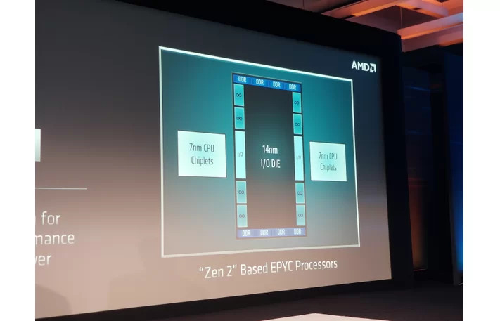
Höchstleistungsrechenzentrum (HLRS, or High-Performance Computing Center), based in Stuttgart Germany, is building a new cluster supercomputer powered by 10,000 AMD Zen 2 "Rome" 64-core processors, making up 640,000 cores. Called "Hawk," the supercomputer will be HLRS' flagship product, and will open its doors to business in 2019. The slide-deck for Hawk makes a fascinating disclosure about the processors it's based on.

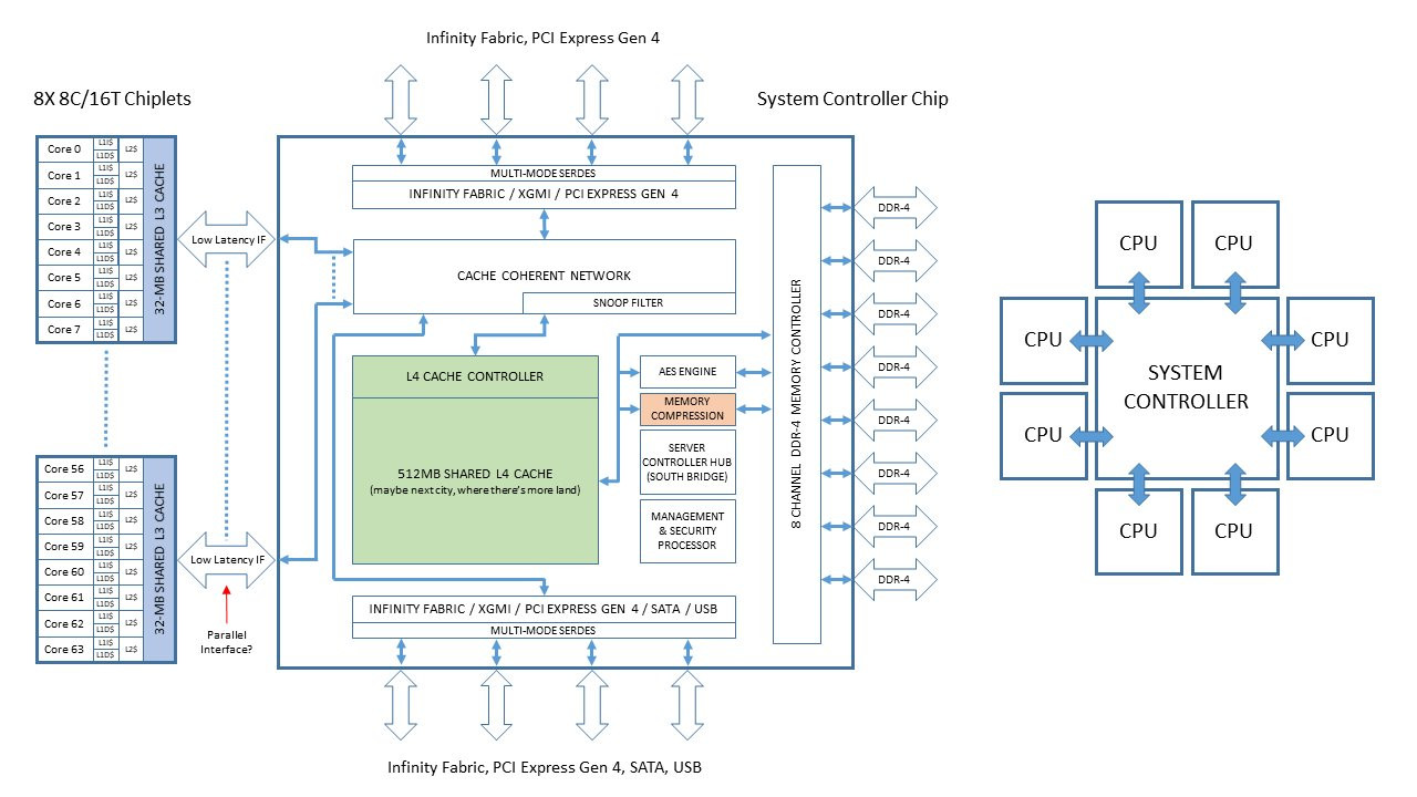
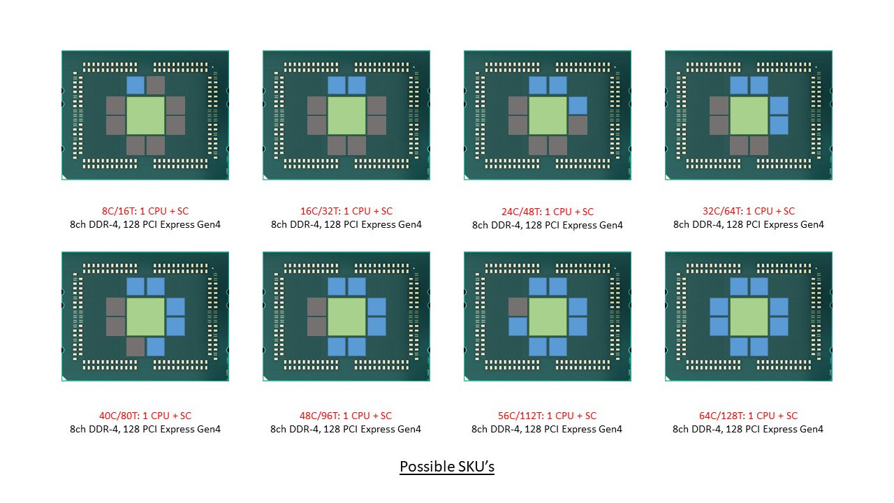
Apparently, each of the 64-core "Rome" EPYC processors has a guaranteed clock-speed of 2.35 GHz. This would mean at maximum load (with all cores loaded 100%), the processor can manage to run at 2.35 GHz. This is important, because the supercomputer's advertised throughput is calculated on this basis, and clients draw up SLAs on throughput. The advertised peak throughput for the whole system is 24.06 petaFLOP/s, although the company is yet to put out nominal/guaranteed performance numbers (which it will only after first-hand testing). The system features 665 TB of RAM, and 26,000 TB of storage.

AMD "Zen 2" IPC 29 Percent Higher than "Zen"

AMD reportedly put out its IPC (instructions per clock) performance guidance for its upcoming "Zen 2" micro-architecture in a version of its Next Horizon investor meeting, and the numbers are staggering. The next-generation CPU architecture provides a massive 29 percent IPC uplift over the original "Zen" architecture. While not developed for the enterprise segment, the stopgap "Zen+" architecture brought about 3-5 percent IPC uplifts over "Zen" on the backs of faster on-die caches and improved Precision Boost algorithms. "Zen 2" is being developed for the 7 nm silicon fabrication process, and on the "Rome" MCM, is part of the 8-core chiplets that aren't subdivided into CCX (8 cores per CCX).

According to Expreview, AMD conducted DKERN + RSA test for integer and floating point units, to arrive at a performance index of 4.53, compared to 3.5 of first-generation Zen, which is a 29.4 percent IPC uplift (loosely interchangeable with single-core performance). "Zen 2" goes a step beyond "Zen+," with its designers turning their attention to critical components that contribute significantly toward IPC - the core's front-end, and the number-crunching machinery, FPU. The front-end of "Zen" and "Zen+" cores are believed to be refinements of previous-generation architectures such as "Excavator." Zen 2 gets a brand-new front-end that's better optimized to distribute and collect workloads between the various on-die components of the core. The number-crunching machinery gets bolstered by 256-bit FPUs, and generally wider execution pipelines and windows. These come together yielding the IPC uplift. "Zen 2" will get its first commercial outing with AMD's 2nd generation EPYC "Rome" 64-core enterprise processors.

Update Nov 14: AMD has issued the following statement regarding these claims.
As we demonstrated at our Next Horizon event last week, our next-generation AMD EPYC server processor based on the new 'Zen 2' core delivers significant performance improvements as a result of both architectural advances and 7nm process technology. Some news media interpreted a 'Zen 2' comment in the press release footnotes to be a specific IPC uplift claim. The data in the footnote represented the performance improvement in a microbenchmark for a specific financial services workload which benefits from both integer and floating point performance improvements and is not intended to quantify the IPC increase a user should expect to see across a wide range of applications. We will provide additional details on 'Zen 2' IPC improvements, and more importantly how the combination of our next-generation architecture and advanced 7nm process technology deliver more performance per socket, when the products launch.

Intel Puts Out Additional "Cascade Lake" Performance Numbers

Intel late last week put out additional real-world HPC and AI compute performance numbers of its upcoming "Cascade Lake" 2x 48-core (96 cores in total) machine, compared to AMD's EPYC 7601 2x 32-core (64 cores in total) machine. You'll recall that on November 5th, the company put out Linpack, System Triad, and Deep Learning Inference numbers, which are all synthetic benchmarks. In a new set of slides, the company revealed a few real-world HPC/AI application performance numbers, including MIMD Lattice Computation (MILC), Weather Research and Forecasting (WRF), OpenFOAM, NAMD scalable molecular dynamics, and YaSK.

The Intel 96-core setup with 12-channel memory interface belts out up to 1.5X performance in MILC, up to 1.6X in WRF and OpenFOAM, up to 2.1X in NAMD, and up to 3.1X in YASK, compared to an AMD EPYC 7601 2P machine. The company also put out system configuration and disclaimer slides with the usual forward-looking CYA. "Cascake Lake" will be Intel's main competitor to AMD's EPYC "Rome" 64-core 4P-capable processor that comes out by the end of 2018. Intel's product is a multi-chip module of two 24~28 core dies, with a 2x 6-channel DDR4 memory interface.

AMD Zen 2 "Rome" MCM Pictured Up Close

Here is the clearest picture of AMD "Rome," codename for the company's next-generation EPYC socket SP3r2 processor, which is a multi-chip module of 9 chiplets (up from four). While first-generation EPYC MCMs (and Ryzen Threadripper) were essentially "4P-on-a-stick," the new "Rome" MCM takes the concept further, by introducing a new centralized uncore component called the I/O die. Up to eight 7 nm "Zen 2" CPU dies surround this large 14 nm die, and connect to it via substrate, using InfinityFabric, without needing a silicon interposer. Each CPU chiplet features 8 cores, and hence we have 64 cores in total.

The CPU dies themselves are significantly smaller than current-generation "Zeppelin" dies, although looking at their size, we're not sure if they're packing disabled integrated memory controllers or PCIe roots anymore. While the transition to 7 nm can be expected to significantly reduce die size, groups of two dies appear to be making up the die-area of a single "Zeppelin." It's possible that the CPU chiplets in "Rome" physically lack an integrated northbridge and southbridge, and only feature a broad InfinityFabric interface. The I/O die handles memory, PCIe, and southbridge functions, featuring an 8-channel DDR4 memory interface that's as monolithic as Intel's implementations, a PCI-Express gen 4.0 root-complex, and other I/O.

AMD Unveils "Zen 2" CPU Architecture and 7 nm Vega Radeon Instinct MI60 at New Horizon

AMD today held its "New Horizon" event for investors, offering guidance and "color" on what the company's near-future could look like. At the event, the company formally launched its Radeon Instinct MI60 GPU-based compute accelerator; and disclosed a few interesting tidbits on its next-generation "Zen 2" mircroarchitecture. The Instinct MI60 is the world's first GPU built on the 7 nanometer silicon fabrication process, and among the first commercially available products built on 7 nm. "Rome" is on track to becoming the first 7 nm processor, and is based on the Zen 2 architecture.

The Radeon Instinct MI60 is based on a 7 nm rendition of the "Vega" architecture. It is not an optical shrink of "Vega 10," and could have more number-crunching machinery, and an HBM2 memory interface that's twice as wide that can hold double the memory. It also features on-die logic that gives it hardware virtualization, which could be a boon for cloud-computing providers.

AMD Could Solve Memory Bottlenecks of its MCM CPUs by Disintegrating the Northbridge

AMD sprung back to competitiveness in the datacenter market with its EPYC enterprise processors, which are multi-chip modules of up to four 8-core dies. Each die has its own integrated northbridge, which controls 2-channel DDR4 memory, and a 32-lane PCI-Express gen 3.0 root complex. In applications that can not only utilize more cores, but also that are memory bandwidth intensive, this approach to non-localized memory presents design bottlenecks. The Ryzen Threadripper WX family highlights many of these bottlenecks, where video encoding benchmarks that are memory-intensive see performance drops as dies without direct access to I/O are starved of memory bandwidth. AMD's solution to this problem is by designing CPU dies with a disabled northbridge (the part of the die with memory controllers and PCIe root complex). This solution could be implemented in its upcoming 2nd generation EPYC processors, codenamed "Rome."

With its "Zen 2" generation, AMD could develop CPU dies in which the integrated northrbidge can be completely disabled (just like the "compute dies" on Threadripper WX processors, which don't have direct memory/PCIe access relying entirely on InfinityFabric). These dies talk to an external die called "System Controller" over a broader InfinityFabric interface. AMD's next-generation MCMs could see a centralized System Controller die that's surrounded by CPU dies, which could all be sitting on a silicon interposer, the same kind found on "Vega 10" and "Fiji" GPUs. An interposer is a silicon die that facilitates high-density microscopic wiring between dies in an MCM. These explosive speculative details and more were put out by Singapore-based @chiakokhua, aka The Retired Engineer, a retired VLSI engineer, who drew block diagrams himself.
Return to Keyword Browsing
May 21st, 2024 09:38 EDT change timezone

New Forum Posts

Popular Reviews

Controversial News Posts