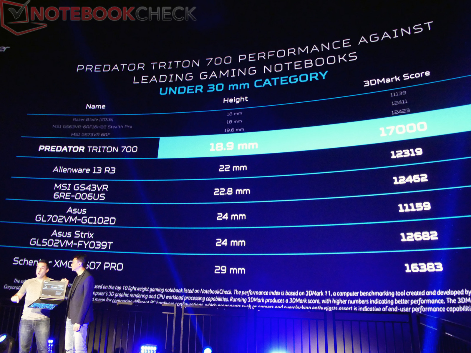
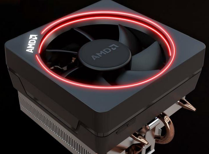
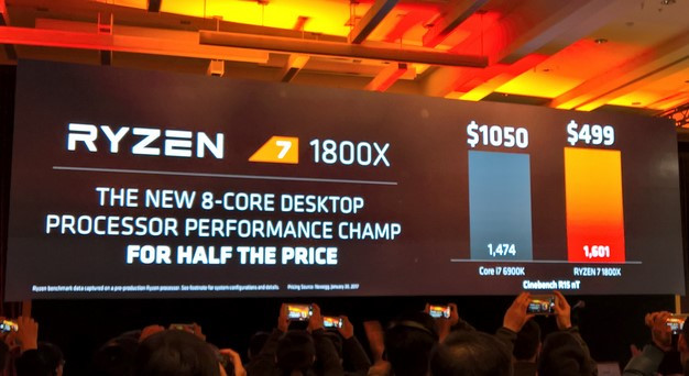
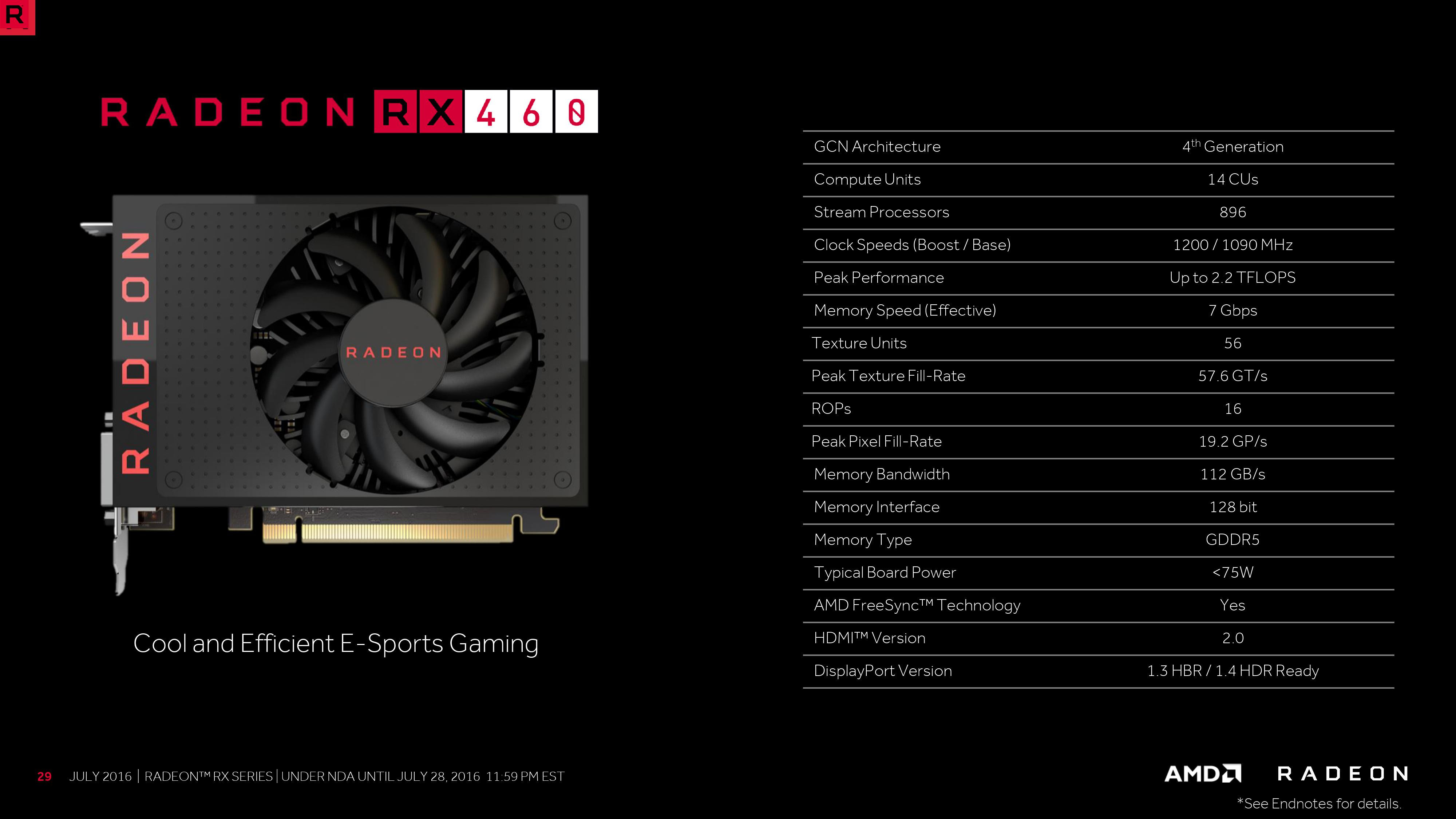
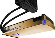
Liquid Cooled AMD Radeon Vega Frontier Edition Now on Sale for $1,489.99
The liquid cooled version of AMD's latest graphics card meant for the "pioneering crowd" of prosumers has been made available over at SabrePC. It sports the exact same GPU you'd find on the air-cooled version, featuring all the same 4096 Stream Processors and 16 GB of HBM2 memory. The only differences are, and you guessed it, the higher cooling capacity afforded by the AIO solution, and the therefore increased TDP from the 300 W of the air-cooled version to a eyebrow-raising 375 W. That increase in TDP must come partially from the employed cooling solution, but also from an (for now, anecdotal) ability for the card to more easily sustain higher clocks, closer to its AMD-rated 1,630 MHz peak core clock.
You can nab one right now in that rather striking gold and blue color scheme, and have it shipped to you in 24H. Hit the source link for the SabrePC page.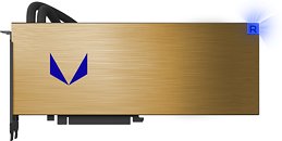

You can nab one right now in that rather striking gold and blue color scheme, and have it shipped to you in 24H. Hit the source link for the SabrePC page.