News Posts matching #Westmere

Return to Keyword Browsing

Moore's Law Buckles as Intel's Tick-Tock Cycle Slows Down

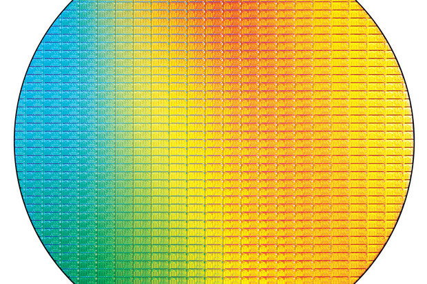
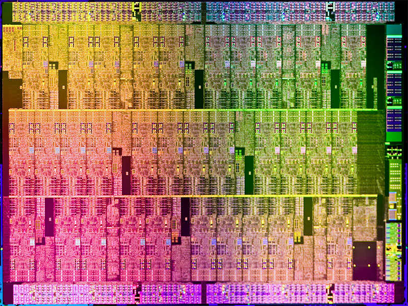
Intel co-founder Gordon Moore's claim that transistor counts in microprocessors can be doubled with 2 years, by means of miniaturizing silicon lithography is beginning to buckle. In its latest earnings release, CEO Brian Krzanich said that the company's recent product cycles marked a slowing down of its "tick-tock" product development from 2 years to close to 2.5 years. With the company approaching sub-10 nm scales, it's bound to stay that way.

To keep Moore's Law alive, Intel adopted a product development strategy it calls tick-tock. Think of it as a metronome that give rhythm to the company. Each "tock" marks the arrival of a new micro-architecture, and each "tick" marks its miniaturization to a smaller silicon fab process. Normally, each year is bound to see one of the two in alternation.

AMD to Emphasize on "Generation" with Future CPU Branding

AMD is planning to play a neat branding game with Intel. Branding of the company's 2016 lineup of CPUs and APUs will emphasize on "generation," much in the same way Intel does with its Core processor family. AMD will mention in its PIB product packaging, OEM specs sheets, and even its product logo (down to the case-badge), that its 2016 products (FX-series CPUs and A-series APUs) are the company's "6th generation." 2016 marks prevalence of Intel's Core "Skylake" processor family, which is its 6th generation Core family (succeeding Nehalem/Westmere, Sandy Bridge, Ivy Bridge, Haswell, and Broadwell). AMD is arriving at its "6th generation" moniker counting "Stars," "Bulldozer," "Piledriver," "Steamroller," and "Excavator," driving its past 5 generations of APUs, and the occasional FX CPU.

It turns out that the emphasis on "generation" is big with DIY and SI retail channels. Retailers we spoke with, say that they find it easier to break through Intel's often-confusing CPU socket change cycle, which ticks roughly every 18-24 months. Customers, they say, find it easier to simply mention the "generation" of Core processor they want, to get all relevant components to go with them (such as motherboard and memory bundles). While AMD's FX brand clearly didn't see generations beyond "Piledriver," the company's decision to unify the socket for its FX and A-Series product lines next year, with AM4, makes "6th generation FX processor" valid.

Intel Ivy Bridge-E Slated for Q3-2013

Intel's next high-end desktop (HEDT) platform, codenamed "Ivy Bridge-E," is slated for Q3-2013, according to the latest platform road-map slide sourced by VR-Zone. According to the leaked slide, launch of Ivy Bridge-E Core i7 processors follows that of Core "Haswell" socket LGA1150 processors (Q2-2013). What's more, the upcoming Ivy Bridge-E chips will be compatible with existing socket LGA2011 motherboards, based on Intel X79 Express chipset.

Intel's next-generation Ivy Bridge-E chips are up-scaled versions of today's Core "Ivy Bridge" chips, built on the same 22 nm process, with more processing cores, memory channels, cache, and PCI-Express 3.0 certified system interfaces. It remains to be seen if Intel launches a new chipset to go with the new processor, or retains the X79 chipset with a few minor updates in the form of steppings. The company retained its X58 Express chipset over the first two HEDT processor generations (45 nm Core i7 "Bloomfield" and 32 nm Core i7 "Westmere").

TYAN Deploys a Series of High-density, Cost-Effective Platforms for Cloud Computing

TYAN offers numerous products for the cloud computing marketplace, including high-density computing, high-density storage, and virtualization environments. TYAN's diverse portfolio provides customers robust options for reducing capital construction and operation costs while offering higher scalability with enhanced performance and energy efficiency.

Intel Xeon E5-2690 Sandy Bridge-EP Performance Leaked

We sourced a presentation, allegedly by Intel, detailing its Sandy Bridge-EP platform, and giving out early performance figures. After successful and trouble-free launches of its Sandy Bridge architecture across all PC form-factors, including the recently-launched Core i7 "Sandy Bridge-E" HEDT (high-end desktop), Intel is taking the architecture to its ultimate market, enterprise, where processors derived from it will make up new lines of Intel Xeon processor families. Intel has two branches of enterprise variations the architecture, Sandy Bridge-EN, designed for high-density, low-power servers, and Sandy Bridge-EP, designed for high-performance servers and workstations. Sandy Bridge-EP is multi-socket capable.

Sandy Bridge-EP uses essentially the same piece of silicon as Sandy Bridge-E, but enabled with several of its features otherwise off limits to the Core processor family. These include twoQuickPath Interconnect (QPI) links, which facilitate high-bandwidth inter-socket communication in multi-socket systems, up to eight cores, sixteen threads enabled by HyperThreading, and up to 20 MB of L3 cache memory. Like its Core family cousins, Xeon Sandy Bridge-EP packs a quad-channel DDR3 integrated memory controller, and PC3-12800 (DDR3-1600 MHz) is its optimal memory standard, but unlike it, supporting up to 768 GB of memory (by two sockets, eight DDR3 channels in all, LRDIMMs). Other key features are listed in the first slide below.
Performance figures follow.

Bulldozer Beats Politicians As The Biggest Fail

On our front page, we placed a poll in mid-September, ahead of AMD FX Processor family launch (based on the "Bulldozer" architecture). Based on the most plausible specifications and the hype surrounding the products at the time, we had a hunch that neither Bulldozer nor Sandy Bridge-E will meet our readers' expectations. AMD FX Processor family turned out to be a Duke Nukem Forever, clogged in the pipeline for too long (since 2007, as a matter of fact), when it came out, it made a mockery of itself. It's barely faster than its previous generation.

Sandy Bridge-E promised to be a pin-up processor platform that's eons faster than its predecessor, its specs-sheets warranted its hype. As it turns out, although they're the fastest processors, they aren't much faster than previous-generation Westmere six-core chips at multi-threaded applications, and aren't much faster than Sandy Bridge LGA1155 Core i7 processors at gaming and serial loads. We set out to find out which would turn out to be a bigger "fail" (failure, in internet jargon). To stuff the poll up with more options, we experimented with the idea of placing a seemingly-unbeatable poll option "Our Politicians", just to see if either of the two could fail so hard, that politicians end up better. The myth that politicians always win at a failing contest is busted, at least in this case.

Intel Aims at 10 nm Processors by 2018

It's not just host nations of the Olympics that are decided almost decades in advance, but also Intel's silicon names and the fab process they're going to be built on. Intel has its plan for the greater part of this decade already charted out, well beyond the upcoming Ivy Bridge architecture. Intel follows the "tick-tock" product cycle, where every micro-architecture gets to be built on two succeeding fab processes, and every fab process getting to have two succeeding micro-architectures built on it, in succession. Westmere is an optical shrink of the Nehalem architecture, it was a "tick" for the 32 nm process, Sandy Bridge is its "tock", and a new architecture. Ivy Bridge is essentially an optical shrink of Sandy Bridge, it is the "tick" for 22 nm process.

Ivy Bridge will make its entry through the LGA1155 platform in 2012, it will make up the 2012 Core processor family. Haswell is the next-generation architecture that succeeds Sandy Bridge and IvyBridge, it will be built on the 22 nm process, and is expected to arrive in 2013. Roswell is its optical shrink to 14 nm, slated for 2014. Looking deep into the decade, there's Skylake architecture, that will span across 14 nm and 10 nm processes with Skymont. This model ensures that Intel has to upgrade its fabs every 2 or so years, an entirely new micro-architecture every 2 or so years as well, while providing optical shrinks every alternating year. Optical shrinks introduce new features, increased caches, and allow higher clock speeds. 10 nm for processors by 2018 sounds realistic looking at the advancement of NAND flash technologies that are pushing the boundaries of fab process development. NAND flash is much less complex than processor development, and hence serve as good precursors to a new process.

Core i7-980 Released at US $583

As reported last week, Intel released its new Core i7-980 six-core processor to the retail channel. The new chip is priced at US $583 in 1000-unit tray quantities, displacing the Core i7-970 from this exact price point it previously held. It is expected that the i7-970 could eventually become cheaper while the platform is still in the market. The Core i7-980 is a socket LGA1366 six-core processor based on the 32 nm "Westmere" silicon. It is clocked at 3.33 GHz, with Turbo Boost speeds of up to 3.60 GHz. Unlike the Core i7-980X Extreme Edition, this chip has an upwards locked BClk multiplier, and its QPI link runs at 4.80 GT/s instead of 6.40 GT/s on the 980X Extreme Edition. As a trade off, the new chip is a little over half the price of the 980X Extreme Edition, which retailed for around US $999.

TYAN Validates Fusion-io 160GB and 640GB ioDrives in Dual-Socket Server Platforms

TYAN, an industry-leading server platform manufacturer, and a subsidiary of MiTAC International Corp., has completed validating 160GB and 640GB ioDrives from Fusion-io in two of their most powerful HPC computing platforms: the S7025, a dual Socket 1366 motherboard supporting Intel Xeon 5500/5600 series processors, and the S8232, the company's newest dual Socket G34 board supporting AMD Opteron 6100 series processors.

TYAN's rigorous validation process included testing ioMemory technology from Fusion-io with a full range of operating systems and applications, as well as comprehensive hardware testing to ensure complete compatibility. Tyan engineers also performed some cursory benchmark tests. "Validating Fusion ioDrives with Tyan's leading HPC platforms gives Tyan and our OEM partners total confidence in Fusion's game changing technology. We're looking forward to expanding our relations with Fusion-io in the future," stated TYAN's Senior Director of Sales, Joe James. Both motherboards are available now through TYAN distributors worldwide. OEM pricing is available on request.

Intel Readies New Xeon X5690 Processor, Fastest Six-Core

Intel is readying its fastest six-core processors ever. While the company is working to introduce the Core i7 990X Extreme Edition for launch sometime in Q4 2010, it's already begun sampling the Xeon X5690. The X5690 is a dual-socket ready LGA1366 processor based on the 32 nm Westmere-EP silicon. It carries a nominal clock-speed of 3.46 GHz (26.0 x 133 MHz), with a Turbo Boost speed of 3.60 GHz (27.0 x 133 MHz). It features a QuickPath Interconnect speed of 6.4 GT/s, and supports triple-channel registered DDR3 memory with its integrated memory controller. Cache levels include 256 KB L2 cache per core, and 12 MB shared L3 cache.

The processor is compatible with most server boards based on the Intel 5500 and 5520 chipsets with BIOS updates. A quick overclocking feat by Fitseries3 on the EVGA Classified SR-2 motherboard yielded a speed of 5 GHz making use of the high BClk multiplier. The chip is likely to carry a rated TDP of 130W. Intel may release this processor in the next quarter, either displacing the X5680 from its US $1,730 price point, or occupying a higher one. The CPU-Z validation of the mentioned overclocking feat can be found here.

Intel Sandy Bridge Quad-Core Processor Tested

At this year's Computex event, some of the most unexpected exhibits were socket LGA1155 motherboards based on Intel 6-series chipsets, across the board, from virtually every major motherboard vendor. Unexpected, because it's been less than an year since released mainstream derivatives of the Nehalem/Westmere architectures that use the LGA1156 socket. LGA1155 will form the base for performance, mainstream, and value segments of processors based on the upcoming Sandy Bridge architecture, which is a generation successor of Nehalem. With so many motherboard vendors showing off their creations in release-grade conditions, it is obvious that engineering samples of processors to go with them are already on the loose and will land in some enthusiast's hands. It did, in the skillful hands of Coolaler, who wasted no time in putting it through a quick run through popular benchmarks.

Coolaler tested an LGA1155 quad-core processor operating at 2.5 GHz, which CPU-Z can't name but marks it as a Sandy Bridge engineering sample. Among the little that's known about this processor, is that it has a base clock speed of 100 MHz (Nehalem/Westmere processors use BClk of 133 MHz), which means that to achieve 2.5 GHz, it uses a multiplier value of 25. It has all the instruction sets of Westmere including SSE 4.2 and AES acceleration, but also features AVX (Advanced Vector Extensions), a successor to SSE 4.2 which expands the processor's number crunching abilities, and increases performance per MHz. The cache structure up to the second level is the same (32 KB L1I, 32 KB L1D, 256 KB /core L2), but uses a smaller L3 cache at 6 MB (compared to 8 MB on Lynnfield). HyperThreading technology provides the OS with 8 logical CPUs to deal with.

Intel Unveils New Product Plans for High-Performance Computing

During the International Supercomputing Conference (ISC), Intel Corporation announced plans to deliver new products based on the Intel Many Integrated Core (MIC) architecture that will create platforms running at trillions of calculations per second, while also retaining the benefits of standard Intel processors.

Targeting high-performance computing segments such as exploration, scientific research and financial or climate simulation, the first product, codenamed "Knights Corner," will be made on Intel's 22-nanometer manufacturing (nm) process - using transistor structures as small as 22 billionths of a meter - and will use Moore's Law to scale to more than 50 Intel processing cores on a single chip. While the vast majority of workloads will still run best on award-winning Intel Xeon processors, Intel MIC architecture will help accelerate select highly parallel applications.

A-Data Low-Voltage Server Memory Gets Westmere-EP Certification

A-DATA Technology Co., Ltd., the worldwide leading manufacturer in high-performance DRAM modules and flash application products, today announced its DDR3L ("L" for low voltage) 1066/1333 (1.35volt) MHz Registered DIMM and DDR3L 1066/1333 MHz (1.35volt) ECC DIMM low voltage server memories have been certified by Intel, that able to perform lower power consumption with great reliability to increase better efficiency on Westmere-EP processor-based server.

"Enterprise often requires 24x7 operations from server memory for data accessing and collecting with reliability and performance requirements," said Richard Shen, manager of A-DATA product management department. "We are proud to offer our DDR3L 1066/1333 MHz R-DIMM and DDR3L 1066/1333 MHz ECC DIMM low voltage server memory that has certified by Intel to enterprise customers, which delivers high performance and great reliability with less power consumption to meet enterprise's critical requirements, as well as to protect and to preserve the environment."

Kingston Technology Releases 1.35V Registered DDR3L Memory Modules Validated by Intel

Kingston Technology Europe Ltd, a subsidiary of Kingston Technology Company, the independent world leader in memory products,today announced that its low-voltage registered dual inline memory modules (RDIMMs) have been validated for use in the upcoming Intel Westmere-EP processor-based server platforms. The Kingston ValueRAM DDR3L ('L' for low voltage) 1333MHz (1.35 volt) server RDIMMs were certified on Intel's Westmere reference platform.

Kingston is proud to offer customers our 1.35-volt server memory and having it certified for use with Intel's next-generation Xeon processors," said Stephane Rizzetto European Product Development Manager for DRAM of Kingston Technology. "Our low voltage registered server memory helps lower total cost of ownership in datacenters as it uses less power, thus producing less heat than equivalent 1.5-volt modules resulting in lower cooling costs for memory-dense servers."

Intel Lets Loose Core i7 980X Performance Evaluations

On the occasion of Game Developers Conference, an annual conclave of game developers, in San Fransisco, USA, Intel previewed to audiences its latest Core i7 980X Extreme Edition six-core processor. This meant that the media could publish performance evaluations of the new processor. Intel seems to have pulled it off with this launch. There is a broad consensus among the media that the six-core processor has a performance incentive with most of today's multi-threaded application that scales up well compared to quad-core processors.

The 980X is also the first high-performance processor based on the 32 nm Westmere architecture. The processor is able to maintain a TDP rating of 130W, on par with its 45 nm Nehalem quad-core counterparts. It has six cores operating at 3.33 GHz, with HyperThreading technology enabled, there are 12 logical CPUs (threads) for the operating system to deal with. Each core has 64 KB L1, 256 KB L2 caches, while a large 12 MB L3 cache is shared between all the cores. The Core i7 980X comes in the LGA-1366 package. Most existing motherboards with the Intel X58 Express chipset will be able to support it with a BIOS update. Intel will formally release the processor by April, at an estimated price of US $999.

Intel to Introduce 8-core Xeon Nehalem-EX, 6-core Westmere-EP Processors This Month

Intel is set to introduce a series of eight-core Xeon server processors later this month, that are capable of running in four-socket servers. With HyperThreading technology enabled, each core can handle two threads, taking the logical CPU count on such servers up to 64. Each Nehalem-EX chip has 8 CPU cores with dedicated L2 caches of 256 KB, a shared L3 cache of 24 MB, and Turbo Boost technology that helps conserve power while also stepping up performance when needed. The die also features a memory controller with four DDR3 memory channels. Being based on the Nehalem architecture, the chips are built on the 45 nm HKMG process.

In related news, Intel will also introduce Westmere-EP processors later this month. These chips will be based on the 32 nm Westmere architecture, and are likely to have 6 cores, up to 12 logical CPUs per chip, 12 MB of L3 cache and three DDR3 memory channels. These chips will be suited for two-socket servers and workstations.

EVGA Names and Details its Dual-LGA1366 Enthusiast Motherboard

EVGA today named its dual-LGA1366 enthusiast-grade motherboard, so far known by the codename W555. After a short contest on the company's forums, the company came up with "EVGA Classified SR-2" for its name. SR stands for "super record" and 2 denoting the dual-socket design. The Classified SR-2 is a an entusiast-grade (read: overclocker friendly) implementation of the Tylersburg platform, supporting Intel socket LGA1366 processors with two QPI links (2P Xeon, etc.) As an addition, the board allows you to do something that's difficult on typical 2P server motherboards: it allows you to mix different models of Xeon processors, provided they're based on the same architecture, and series. For example, you can mix a Xeon 5520 with Xeon 5540. You can also mix a quad-core processor with a six-core processor, provided the quad-core part is based on the Westmere architecture (32 nm), not Nehalem (45 nm).

The board will also let you run a single 2P-capable processor in either sockets. DDR3 memory modules can be non-ECC or even ECC. 2P Xeon DRAM Multipliers / Uncore Multipliers are locked so you will only be able to use maximum 2:8 or 2:10 depending on segment of CPU. EVGA tells that the board supports 4-way SLI on its GTX 285 Classified VGA, but adds that a "future flagship GPU" also supports it. Could this be GeForce GTX 400 series having it as a standard feature? We have to wait and see. 4-way CrossFireX is supported.

ASUS Rampage III Extreme Smiles for the Camera

One of ASUS' premier offers for this year's Consumer Electronics Show (CES) event is a new high-end socket LGA-1366 motherboard, the Republic of Gamers (ROG) Rampage III Extreme. The board succeeds the Rampage II Extreme which launched over an year ago along with Intel's then new Core i7 series processors. The new model based on the Intel X58 Express + ICH10R chipset, comes with four well spaced out PCI-Express 2.0 x16 slots, a new set of overclocking enhancements such as the ROG connect which lets you control the motherboard's overclocking from any Bluetooth and Java enabled mobile phone, SATA 6 Gb/s and USB 3.0 connectivity using ASUS' innovative PCI-Express 2.0 bridge implementation, and a more powerful CPU VRM to keep the board stable with bleeding-edge settings.

The board features an enhanced CPU VRM which is now powered by two 8-pin ATX connectors apart from two 4-pin Molex connectors. Some of these could be redundant and needed only for electrical stability. The CPU and memory power circuitry makes use of super-ML capacitors for cleaner power delivery. Voltage readouts are located next to the DIMM slots for accessibility. The motherboard makes use of slimmer component heatsinks that look to be made of the ceramic composite which the TUF Sabertooth P55 motherboard uses.

Intel Unveils Core i5 6xx, 6x1 Series Dual-Core Processors

Intel today gave a go ahead for the media to publish reviews of its brand new dual-core processors under the Core i5 6xx and Core i5 6x1 series. The processors are based on the new "Clarkdale" processor die, and make use of the company's 32 nm next generation HKMG manufacturing process. Unlike conventional processor packages based on the Nehalem/Westmere architecture, the new processors move the northbridge component of the system onto the processor package, only that it is based on a separate 45 nm die within the package. The 32 nm processor die houses two processor cores along with up to 4 MB of L3 cache, while it is wired to a larger iGPU die which houses the dual-channel DDR3 memory controller, a graphics core, PCI-Express root complex, along with other components traditionally found on northbridge chips.

The first three models in the new Core i5 series are the 3.20 GHz Core i5 650, 3.33 GHz Core i5 660 and 661 (latter has a faster iGPU), and 3.46 GHz Core i5 670. These processors have the LGA-1156 package and are compatible with existing P55 Express chipset (albeit without the iGPU feature), along with the company's new H55 Express and H57 Express chipsets that support the Flexible Display Interface that provides connectivity to the processors' iGPUs. The new processors feature HyperThreading Technology, with which it provides the operating system with four logical CPUs (threads) to deal with, TurboBoost technology which powers down a core and overclocks the other when the task load is low. Pricing and availability will surface when the processors are formally announced, a little later this month. Meanwhile, motherboard manufacturers are ready with boatloads of new motherboard models based on Intel's two new chipsets. A compilation of links to major reviews on the internet can be found in the day's reviews list on the homepage.

Intel Readies 13 Westmere-based 32 nm Xeon Processors

Outgrowing the known lineup of 32 nm client processors (under the Core family), Intel's upcoming lineup of processors based on the 32 nm Westmere architecture will comprise of no less than 13 models under the Xeon E5000, L5000, X5000, and W3600 series. Among these, there are six hexa-core Xeon processors, including X5680 (3.33 GHz), X5670 (2.93 GHz), X5660 (2.80 GHz), and X5650 (2.66 GHz). X5680 has a TDP of 130W, with the latter three sub 3 GHz models having TDP as low as 95W. There is an energy-efficient L5640 hexa-core model clocked at 2.26 GHz, with TDP at 60W, and a single-socket W3680, clocked at 3.33 GHz with 130W TDP. All these models have six cores, and 12 MB of L3 cache.

Next up, are Intel's first 32 nm quad-core processors: Xeon X5677 (3.46 GHz, 130W), X5647 (3.06 GHz, 95W), E5640 (2.66 GHz, 80W), X5630 (2.53 GHz, 80W), X5620 (2.40 GHz, 80W), and energy efficient L5630 (2.13 GHz, 40W), and L5609 (1.86 GHz, 40W). Except L5609, all these quad-core chips have HyperThreading Technology and Turbo Boost available. The L2 cache amounts for each of these chips is unknown as of now, but should be up to 8 MB, or as low as 4 MB for some models. Most of these chips are slated for release on March 16, 2010.

Intel Commences 32 nm Chip Production

Intel's foundries have commenced mass production of the company's first processors based on the 32 nm second generation high-K metal gate (HKMG) technologies. With these the company's next-generation Westmere architecture becomes retail-grade. The first products will include dual-core processors compatible with the recently introduced socket LGA-1156 platforms, and will carry the brand identifiers (and model number schemes) Core i5 600 series, Core i3 500 series, and Pentium dual-core series.

The desktop-grade parts are based on the "Clarkdale" core, and notebook-grade ones "Arrandale". The latter will be introduced first among the two, with the first Arrandale chips slated for Q4 2009, while the desktop chips arrive a little later in Q1 2010. Intel will focus on this transition to the Westmere architecture in the upcoming Intel Developer Forum event.

Intel Updates Mainstream, Performance, and Extreme CPU Roadmap

Intel issued a confidential roadmap for CPU product releases that looks as far as Q3 2010, leaked to sections of the Chinese media. The roadmap covers prominent Intel processors in their designated market segments drawn out by Intel, covering three grades of mainstream, one each of performance and extreme. The roadmap marks a definite transition of architectures from Intel's Core (penryn) to next-generation Nehalem, and the advent of Intel's first 32 nm based Westmere CPUs.

To begin with, there three models of Intel's first LGA-1156 processors scheduled for Q3 2009, the quad-core "Lynnfield" based Core i7 870 (2.93 GHz, HTT) in Performance, Core i7 860 (2.80 GHz, HTT) in MS3/upper-mainstream, and Core i5 750 (2.66 GHz, no HTT) in MS2/middle-mainstream. The HTT-enabled Core i7 800 processors were earlier believed to have been scheduled for Q1 2010, but are combined with the Core i5 750 for a grand platform launch. The Core i7 800 models will remain seated in their segments for the better part of 2010.

Core i9 ''Gulftown'' Comes to Life

Intel's posterboy processor for the 32 nm Westmere architecture, the six-core Gulftown is now living, breathing silicon. The company seems to have already dispatched samples of the chip. Gulftown is based on the LGA-1366 socket. Featuring 6 cores and 12 threads with HyperThreading enabled, it holds 12 MB of L3 cache to support the additional data load over the QuickPath Interconnect.

A noted enthusiast has two Gulftown processors running in a dual-socket setup. This 12 core, 24 thread monstrosity uses 24 GB of DDR3 memory using 4 GB modules (perhaps 2 x 3 modules). The processors are running at 2.40 GHz (18 x 133 MHz). The machine was put through WPrime multi-threaded benchmark. It crunched WPrime 32M in a little over 6 seconds, and 1024M in 145.6 seconds. Going by older information, Gulftown should be implemented in a commercial product in Q1 2010, when Intel plans a host of other important product launches. When released as Core i9, the processor will target the premium enthusiast market.

Clarkdale 3.06 GHz Faces a Preview, Series Pricing Surfaces

"Clarkdale" is the codename for Intel's upcoming dual-core processors derived from the Nehalem/Westmere architecture. The move marks a leap for Intel in two ways: introducting the first commercial-grade 32 nm microprocessor, and implementing a radical new design that involved relocating the platform's northbridge component entirely to the CPU package. Slated for Q1 2010, Clarkdale will go by three brand indentifiers to grade it according to a performance and feature scale. You have the Core i5 class that enables the entire feature-set of processor, there's the Core i3 class that offers some features, excluding Intel Turbo Boost technology for example, finally there's the sub-$100 Pentium part (yes, Pentium lives on), which offers a smaller feature-set. HyperThreading technology is disabled on this one.

Chinese tech-site IT168 published a comprehensive performance (p)review of the 3.06 GHz Clarkdale part. In the article, the 3.06 GHz Clarkdale was pitted against the 3.00 GHz "Wolfdale" Core 2 Duo processor. The memory (Dual-channel DDR3-1333, 4 GB) and graphics hardware (ATI Radeon HD 4870, 1 GB) were kept common between the two test-beds. Tests ranged from memory and CPU internal bandwidth tests, math-intensive tests, synthetic multimedia and 3D tests, and finally, modern 3D games.

First Intel Clarkdale Core i3 Low-Voltage Overclocking Feat Yields 4 GHz at 0.832 V

Intel's upcoming dual-core derivatives of the Nehalem/Westmere architecture, codenamed "Clarkdale" seems to have some interesting electrical characteristics. The CPU component of the chip is built on Intel's brand new 32 nanometre process that facilitates higher transistor densities, and in the process, intends to bring down TDP. An overclocking feat by Coolaler.com seems to suggest one of two things: either these chips have naturally low vCore voltages, or that the overlocking headroom at low-voltages is exceptional. Coolaler used a pre-release engineering sample of the Core i3 Clarkdale processor on a compatible platform, and achieved 4 GHz of clock speed with the vCore at 0.832 V. The frequency multiplier of the CPU was set at 25.0x, and a bus speed of 160 MHz used. Intel will be ready with these processors by the end of this year.
Return to Keyword Browsing
May 2nd, 2024 02:51 EDT change timezone

New Forum Posts

Popular Reviews

Controversial News Posts