News Posts matching #Xilinx

Return to Keyword Browsing

Xilinx Announces World's Highest Bandwidth, Highest Compute Density Adaptable Platform for Network and Cloud Acceleration

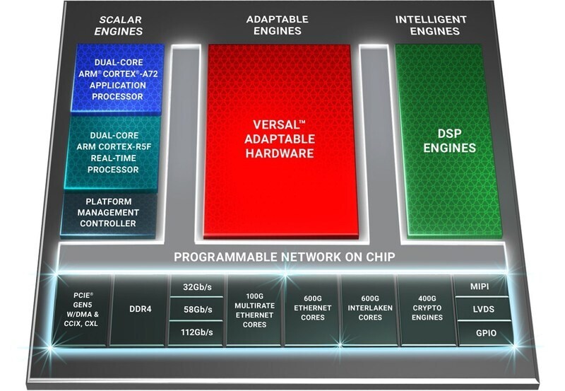
Xilinx, Inc. today announced Versal Premium, the third series in the Versal ACAP portfolio. The Versal Premium series features highly integrated, networked and power-optimized cores and the industry's highest bandwidth and compute density on an adaptable platform. Versal Premium is designed for the highest bandwidth networks operating in thermally and spatially constrained environments, as well as for cloud providers who need scalable, adaptable application acceleration.

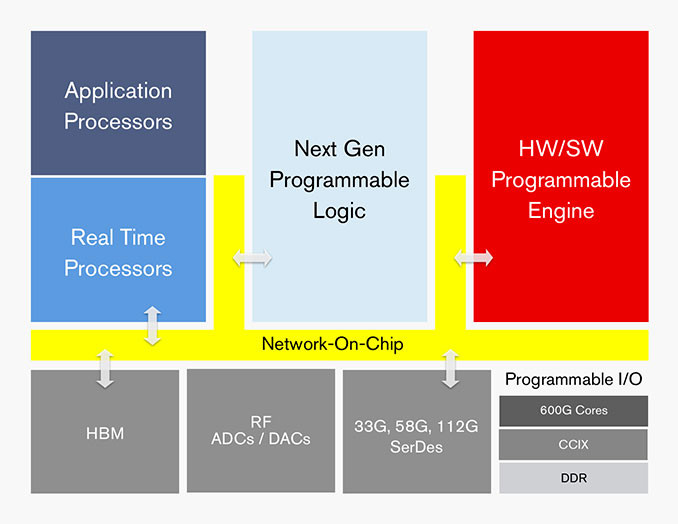
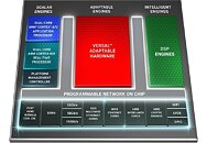
Versal is the industry's first adaptive compute acceleration platform (ACAP), a revolutionary new category of heterogeneous compute devices with capabilities that far exceed those of conventional silicon architectures. Developed on TSMC's 7-nanometer process technology, Versal Premium combines software programmability with dynamically configurable hardware acceleration and pre-engineered connectivity and security features to enable a faster time-to-market. The Versal Premium series delivers up to 3X higher throughput compared to current generation FPGAs, with built-in Ethernet, Interlaken, and cryptographic engines that enable fast and secure networks. The series doubles the compute density of currently deployed mainstream FPGAs and provides the adaptability to keep pace with increasingly diverse and evolving cloud and networking workloads.
Xilinx Versal ACAP FPGA

NVIDIA Leads the Edge AI Chipset Market but Competition is Intensifying: ABI Research

Diversity is the name of the game when it comes to the edge Artificial Intelligence (AI) chipset industry. In 2019, the AI industry is witnessing the continual migration of AI workloads, particularly AI inference, to edge devices, including on-premise servers, gateways, and end-devices and sensors. Based on the AI development in 17 vertical markets, ABI Research, a global tech market advisory firm, estimates that the edge AI chipset market will grow from US $2.6 billion in 2019 to US $7.6 billion by 2024, with no vendor commanding more than 40% of the market.

The frontrunner of this market is NVIDIA, with a 39% revenue share in the first half of 2019. The GPU vendor has a strong presence in key AI verticals that are currently leading in AI deployments, such as automotive, camera systems, robotics, and smart manufacturing. "In the face of different use cases, NVIDIA chooses to release GPU chipsets with different computational and power budgets. In combination with its large developer ecosystem and partnerships with academic and research institutions, the chipset vendor has developed a strong foothold in the edge AI industry," said Lian Jye Su, Principal Analyst at ABI Research.

NVIDIA is facing stiff competition from Intel with its comprehensive chipset portfolio, from Xeon CPU to Mobileye and Movidius Myriad. At the same time, FPGA vendors, such as Xilinx, QuickLogic, and Lattice Semiconductor, are creating compelling solutions for industrial AI applications. One missing vertical from NVIDIA's wide footprint is consumer electronics, specifically smartphones. In recent years, AI processing in smartphones has been driven by smartphone chipset manufacturers and smartphone vendors, such as Qualcomm, Huawei, and Apple. In smart home applications, MediaTek and Amlogic are making their presence known through the widespread adoption of voice control front ends and smart appliances.

Compute Express Link Consortium (CXL) Officially Incorporates

Today, Alibaba, Cisco, Dell EMC, Facebook, Google, Hewlett Packard Enterprise, Huawei, Intel Corporation and Microsoft announce the incorporation of the Compute Express Link (CXL) Consortium, and unveiled the names of its newly-elected members to its Board of Directors. The core group of key industry partners announced their intent to incorporate in March 2019, and remain dedicated to advancing the CXL standard, a new high-speed CPU-to-Device and CPU-to-Memory interconnect which accelerates next-generation data center performance.

The five new CXL board members are as follows: Steve Fields, Fellow and Chief Engineer of Power Systems, IBM; Gaurav Singh, Corporate Vice President, Xilinx; Dong Wei, Standards Architect and Fellow at ARM Holdings; Nathan Kalyanasundharam, Senior Fellow at AMD Semiconductor; and Larrie Carr, Fellow, Technical Strategy and Architecture, Data Center Solutions, Microchip Technology Inc.

Xilinx Announces Virtex UltraScale+, the World's Largest FPGA

Xilinx, Inc., the leader in adaptive and intelligent computing, today announced the expansion of its 16 nanometer (nm) Virtex UltraScale+ family to now include the world's largest FPGA — the Virtex UltraScale+ VU19P. With 35 billion transistors, the VU19P provides the highest logic density and I/O count on a single device ever built, enabling emulation and prototyping of tomorrow's most advanced ASIC and SoC technologies, as well as test, measurement, compute, networking, aerospace and defense-related applications.

The VU19P sets a new standard in FPGAs, featuring 9 million system logic cells, up to 1.5 terabits per-second of DDR4 memory bandwidth and up to 4.5 terabits per-second of transceiver bandwidth, and over 2,000 user I/Os. It enables the prototyping and emulation of today's most complex SoCs as well as the development of emerging, complex algorithms such as those used for artificial intelligence, machine learning, video processing and sensor fusion. The VU19P is 1.6X larger than its predecessor and what was previously the industry's largest FPGA — the 20 nm Virtex UltraScale 440 FPGA.

2nd Gen AMD EPYC Processors Set New Standard for the Modern Datacenter

At a launch event today, AMD was joined by an expansive ecosystem of datacenter partners and customers to introduce the 2nd Generation AMD EPYC family of processors that deliver performance leadership across a broad number of enterprise, cloud and high-performance computing (HPC) workloads. 2nd Gen AMD EPYC processors feature up to 64 "Zen 2" cores in leading-edge 7 nm process technology to deliver record-setting performance while helping reduce total cost of ownership (TCO) by up to 50% across numerous workloads. At the event, Google and Twitter announced new 2nd Gen AMD EPYC processor deployments and HPE and Lenovo announced immediate availability of new platforms.

"Today, we set a new standard for the modern datacenter with the launch of our 2nd Gen AMD EPYC processors that deliver record-setting performance and significantly lower total cost of ownership across a broad set of workloads," said Dr. Lisa Su, president and CEO, AMD. "Adoption of our new leadership server processors is accelerating with multiple new enterprise, cloud and HPC customers choosing EPYC processors to meet their most demanding server computing needs."

Xilinx Introduces HDMI 2.1 IP Subsystem

Xilinx, Inc., the leader in adaptive and intelligent computing, today announced that it has introduced a complete HDMI 2.1 IP subsystem to its portfolio of intellectual property cores, enabling Xilinx devices to transmit, receive and process up to 8K (7680 x 4320 pixels) ultra-high-definition (UHD) video in pro AV equipment, including cameras, streaming media players, professional monitors, LED walls, projectors and KVM, as well as broadcast products such as end points and infrastructure that are being upgraded to handle 8K video.

Customers are increasingly adopting machine learning to monetize and improve workflows in diverse applications such as broadcast, pro AV, automotive and surveillance. HDMI 2.1 data rates are provided by Xilinx's highly reliable high-speed I/O transceivers. This, combined with native 8K interfaces supported by HDMI 2.1 now make it possible to replace several ASSP's or fixed-function products support processing, compression, high-quality analytics and decision-making with a single Xilinx device.

TSMC 7nm EUV Process to Enter Mass-Production in March 2019

TSMC is giving final touches to set its flagship 7 nanometer EUV (extreme ultraviolet lithography) silicon fabrication node at its highest state of readiness for business, called mass-production. At this state, the node can mass-produce products for TSMC's customers. TSMC had taped out its first 7 nm EUV chips in October 2018. The company will also begin risk-production of the more advanced 5 nm node in April, staying on schedule. Mass production of 5 nm chips could commence in the first half of 2020.

The 7 nm EUV node augments TSMC's 7 nm DUV (deep ultraviolet lithography) node that's been already active since April 2018, and producing chips for AMD, Apple, HiSilicon, and Xilinx. At the turn of the year, 7 nm DUV made up 9 percent of TSMC's shipments. With the new node going online, 7 nm (DUV + EUV) could make up 25 percent of TSMC's output by the end of 2019.

AMD and Xilinx Announce a New World Record for AI Inference

At today's Xilinx Developer Forum in San Jose, Calif., our CEO, Victor Peng was joined by the AMD CTO Mark Papermaster for a Guinness. But not the kind that comes in a pint - the kind that comes in a record book. The companies revealed the AMD and Xilinx have been jointly working to connect AMD EPYC CPUs and the new Xilinx Alveo line of acceleration cards for high-performance, real-time AI inference processing. To back it up, they revealed a world-record 30,000 images per-second inference throughput!

The impressive system, which will be featured in the Alveo ecosystem zone at XDF today, leverages two AMD EPYC 7551 server CPUs with its industry-leading PCIe connectivity, along with eight of the freshly-announced Xilinx Alveo U250 acceleration cards. The inference performance is powered by Xilinx ML Suite, which allows developers to optimize and deploy accelerated inference and supports numerous machine learning frameworks such as TensorFlow. The benchmark was performed on GoogLeNet, a widely used convolutional neural network.

Xilinx Unveils Their Revolutionary Adaptive Compute Acceleration Platform

Xilinx, Inc., the leader in adaptive and intelligent computing, today announced a new breakthrough product category called adaptive compute acceleration platform (ACAP) that goes far beyond the capabilities of an FPGA. An ACAP is a highly integrated multi-core heterogeneous compute platform that can be changed at the hardware level to adapt to the needs of a wide range of applications and workloads. An ACAP's adaptability, which can be done dynamically during operation, delivers levels of performance and performance per-watt that is unmatched by CPUs or GPUs.

An ACAP is ideally suited to accelerate a broad set of applications in the emerging era of big data and artificial intelligence. These include: video transcoding, database, data compression, search, AI inference, genomics, machine vision, computational storage and network acceleration. Software and hardware developers will be able to design ACAP-based products for end point, edge and cloud applications. The first ACAP product family, codenamed "Everest," will be developed in TSMC 7nm process technology and will tape out later this year.

AMD Announces the Radeon Instinct Family of Deep-Learning Accelerators

AMD (NASDAQ: AMD) today unveiled its strategy to accelerate the machine intelligence era in server computing through a new suite of hardware
and open-source software offerings designed to dramatically increase performance, efficiency, and ease of implementation of deep learning workloads. New Radeon Instinct accelerators will offer organizations powerful GPU-based solutions for deep learning inference and training. Along with the new hardware offerings, AMD announced MIOpen, a free, open-source library for GPU accelerators intended to enable high-performance machine intelligence implementations, and new, optimized deep learning frameworks on AMD's ROCm software to build the foundation of the next evolution of machine intelligence workloads.

Inexpensive high-capacity storage, an abundance of sensor driven data, and the exponential growth of user-generated content are driving exabytes of data globally. Recent advances in machine intelligence algorithms mapped to high-performance GPUs are enabling orders of magnitude acceleration of the processing and understanding of that data, producing insights in near real time. Radeon Instinct is a blueprint for an open software ecosystem for machine intelligence, helping to speed inference insights and algorithm training.

Industry Leaders Join Forces to Promote New High-Performance Interconnect

A group of leading technology companies today announced the Gen-Z Consortium, an industry alliance working to create and commercialize a new scalable computing interconnect and protocol. This flexible, high-performance memory semantic fabric provides a peer-to-peer interconnect that easily accesses large volumes of data while lowering costs and avoiding today's bottlenecks. The alliance members include AMD, ARM, Cavium Inc., Cray, Dell EMC, Hewlett Packard Enterprise (HPE), Huawei, IBM, IDT, Lenovo, Mellanox Technologies, Micron, Microsemi, Red Hat, Samsung, Seagate, SK hynix, Western Digital Corporation, and Xilinx.

Modern computer systems have been built around the assumption that storage is slow, persistent and reliable, while data in memory is fast but volatile. As new storage class memory technologies emerge that drive the convergence of storage and memory attributes, the programmatic and architectural assumptions that have worked in the past are no longer optimal. The challenges associated with explosive data growth, real-time application demands, the emergence of low latency storage class memory, and demand for rack scale resource pools require a new approach to data access.

Seagate Announces New Alignment of Global Markets & Customers Organization

Seagate Technology plc (NASDAQ: STX), a world leader in storage solutions, today announced that its Global Markets & Customers organization will be aligned under Dave Mosley, President, Operations and Technology, effective immediately. Mr. Mosley will continue to report to Steve Luczo, Chairman and Chief Executive Officer.

"I'm looking forward to working with Dave over the next several years as we continue to optimize Seagate in a way to best serve our expanding global customer base. Seagate's focus on operational efficiency in our global high technology manufacturing facilities and design centers has benefitted our storage technology portfolio, competitive position and financial performance," said Mr. Luczo. "Given these positive results, we are extending this operational efficiency into Seagate's market-facing functions to help further align our structure. We expect the transition to be seamless, as Dave has previously managed Seagate's sales, marketing and product management functions."

Rocky Pimentel, Seagate's President of Global Markets and Customers will remain with the company as Executive Vice President and report to Mr. Luczo. Mr. Pimentel will have responsibility for a number of strategic projects within the company and will continue to serve on selected boards.

TSMC 16FinFET Plus Process Achieves Risk Production Milestone

TSMC today announced its 16-nanometer FinFET Plus (16FF+) process is now in risk production. This enhanced version of TSMC's 16FF process operates 40% faster than the company's planar 20-nanometer system-on-chip (20SoC) process, or consumes 50% less power at the same speed. It offers customers a new level of performance and power optimization targeted at the next generation of high-end mobile, computing, networking, and consumer applications.

TSMC's 16nm process offers an extended scaling of advanced SoC designs and is verified to reach speeds of 2.3GHz with ARM's "big" Cortex-A57 in high-speed applications while consuming as little as 75mW with the "LITTLE" Cortex-A53 in low-power applications. It is making excellent progress in yield learning, and has achieved the best technology maturity at the same corresponding stage as compared to all TSMC's previous nodes.

Hybrid Memory Cube Consortium Finalizes Specifications

More than 100 developer and adopter members of the Hybrid Memory Cube Consortium (HMCC) today announced they've reached consensus for the global standard that will deliver a much-anticipated, disruptive memory computing solution. Developed in only 17 months, the final specification marks the turning point for designers in a wide range of segments-from networking and high-performance computing, to industrial and beyond-to begin designing Hybrid Memory Cube (HMC) technology into future products.

A major breakthrough with HMC is the long-awaited utilization of advanced technologies to combine highperformance logic with state-of-the-art DRAM. With this first HMC milestone reached so quickly, consortium members have elected to extend their collaborative effort to achieve agreement on the next generation of HMC interface standards.

Xilinx 7 Series FPGA/Micron RLDRAM 3 Platform Enables Substantially Higher Data Rates

Xilinx, Inc. and Micron Technology, Inc., today announced the first public hardware demonstration of an FPGA interfacing with RLDRAM 3 memory, a new and emerging memory standard for high-end networking applications such as packet buffering and inspection, linked lists, and lookup tables. Operating with Virtex-7 and Kintex-7 FPGAs at data rates up to 1600 megabits per second (Mb/s), Micron's high-performance RLDRAM 3 memory combines high density, high bandwidth and fast SRAM-like random access to enable a 60 percent higher data rate and memory bandwidth compared to that of the previous generation (Virtex-6 FPGAs/RLDRAM2 memory standard). RLDRAM 3 memory enables 40G and 100G networking systems that require higher speed, higher density, lower power and lower latency.

Virtex-7 and Kintex-7 FPGAs are designed with the necessary IO standards and architectural components for optimal interfacing with RLDRAM 3, providing a significant boost to system performance for high-performance wireless and wired networking systems. RLDRAM 3 memory uses innovative circuit design to minimize the time between the beginning of an access cycle and the instant that the first data is available. Ultra-low bus turnaround time enables higher sustainable bandwidth with near-term balanced read-to-write ratios.
Return to Keyword Browsing
May 21st, 2024 14:28 EDT change timezone

New Forum Posts

Popular Reviews

Controversial News Posts