News Posts matching #chipset

Return to Keyword Browsing

Intel Statement on Stability Issues: "Motherboard Makers to Blame"

A couple of weeks ago, we reported on NVIDIA directing users of Intel's 13th Generation Raptor Lake and 14th Generation Raptor Lake Refresh CPUs to consult Intel for any issues with system stability. Motherboard makers, by default, often run the CPU outside of Intel's recommended specifications, overvolting the CPU through modifying voltage curves, automatic overclocks, and removing power limits.

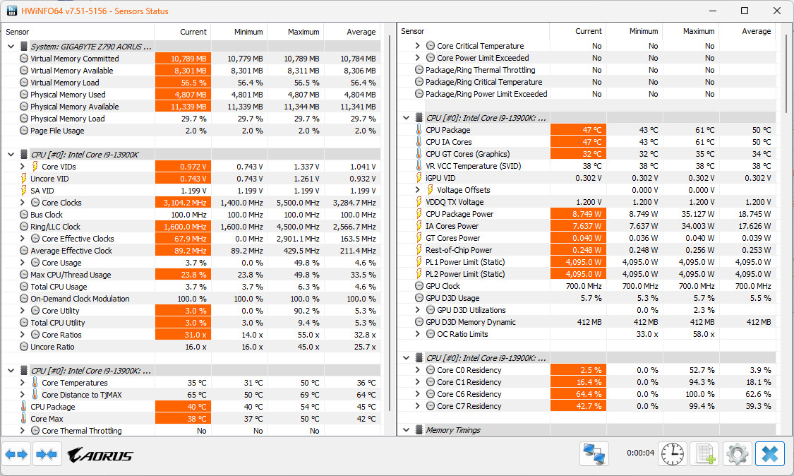
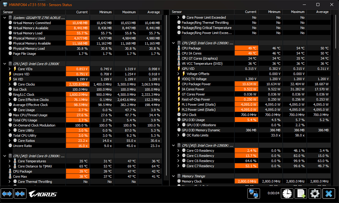
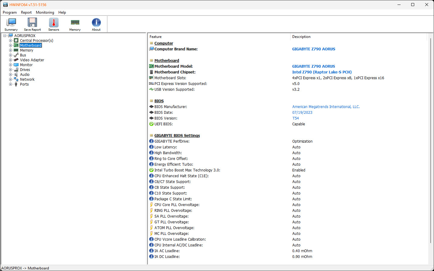
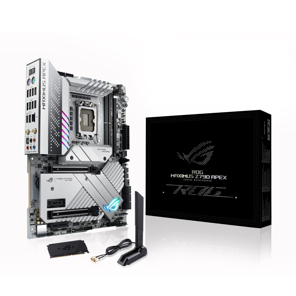
Today, we learned that Igor's Lab has obtained a statement from Intel that the company prepared for motherboard OEMs regarding the issues multiple users report. Intel CPUs come pre-programmed with a stock voltage curve. When motherboard makers remove power limits and automatically adjust voltage curves and frequency targets, the CPU can be pushed outside its safe operating range, possibly causing system instability. Intel has set up a dedicated website for users to report their issues and offer support. Manufacturers like GIGABYTE have already issued new BIOS updates for users to achieve maximum stability, which incidentally has recent user reports of still being outside Intel spec, setting PL2 to 188 W, loadlines to 1.7/1.7 and current limit to 249 A. While MSI provided a blog post tutorial for stability. ASUS has published updated BIOS for its motherboards to reflect on this Intel baseline spec as well. Surprisingly, not all the revised BIOS values match up with the Intel Baseline Profile spec for these various new BIOS updates from different vendors. You can read the statement from Intel in the quote below.

Global Top 10 Foundries Q4 Revenue Up 7.9%, Annual Total Hits US$111.54 Billion in 2023

The latest TrendForce report reveals a notable 7.9% jump in 4Q23 revenue for the world's top ten semiconductor foundries, reaching $30.49 billion. This growth is primarily driven by sustained demand for smartphone components, such as mid and low-end smartphone APs and peripheral PMICs. The launch season for Apple's latest devices also significantly contributed, fueling shipments for the A17 chipset and associated peripheral ICs, including OLED DDIs, CIS, and PMICs. TSMC's premium 3 nm process notably enhanced its revenue contribution, pushing its global market share past the 60% threshold this quarter.

TrendForce remarks that 2023 was a challenging year for foundries, marked by high inventory levels across the supply chain, a weak global economy, and a slow recovery in the Chinese market. These factors led to a downward cycle in the industry, with the top ten foundries experiencing a 13.6% annual drop as revenue reached just $111.54 billion. Nevertheless, 2024 promises a brighter outlook, with AI-driven demand expected to boost annual revenue by 12% to $125.24 billion. TSMC, benefiting from steady advanced process orders, is poised to far exceed the industry average in growth.

SMIC Prepares for 3 nm Node Development, Requires Chinese Government Subsidies

SMIC, China's largest semiconductor manufacturer, is reportedly assembling a dedicated team to develop 3 nm semiconductor node technology, following reports of the company setting up 5 nm chip production for Huawei later this year. This move is part of SMIC's efforts to achieve independence from foreign companies and reduce its reliance on US technology. According to a report from Joongang, SMIC's initial goal is to commence operations of its 5 nm production line, which will mass-produce Huawei chipsets for various products, including AI silicon. However, SMIC is already looking beyond the 5 nm node. The company has assembled an internal research and development team to begin work on the next-generation 3 nm node.

The Chinese manufacturer is expected to accomplish this using existing DUV machinery, as ASML, the sole supplier of advanced EUV technology, is prohibited from providing equipment to Chinese companies due to US restrictions. It is reported that one of the biggest challenges facing SMIC is the potential for low yields and high production costs. The company is seeking substantial subsidies from the Chinese government to overcome these obstacles. Receiving government subsidies will be crucial for SMIC, especially considering that its 5 nm chips are expected to be up to 50 percent more expensive than TSMC's due to the use of older DUV equipment. The first 3 nm wafers from SMIC are not expected to roll out for several years, as the company will prioritize the commercialization of Huawei's 5 nm chips. This ambitious undertaking by SMIC represents a significant challenge for the company as it strives to reduce its dependence on foreign semiconductor technology and establish itself as an essential player in the global manufacturing industry.

Apple M4 & A18 Chipsets Linked to Significant Neural Engine Upgrade

Apple CEO, Tim Cook, discussed planned generative AI software features during an early February earnings call: "As we look ahead, we will continue to invest in these and other technologies that will shape the future. That includes artificial intelligence, where we continue to spend a tremendous amount of time and effort, and we're excited to share the details of our ongoing work in that space later this year." His "prepared" statement did not provide any specific insights into involved technologies, but many iPhone experts believe that the upcoming release of iOS 18 could be "the biggest update" in Apple mobile operating system history. The American multinational technology giant is seemingly taking a relaxed approach with internal artificial intelligence developments—rival smartphone maker, Samsung, has already jumped into the on-the-go AI deep end with its recently launched Galaxy S24 series. Qualcomm's Snapdragon 8 Gen 3 (for Galaxy) chipset is ready to take on all sorts of artificial intelligence-augmented tasks, while a next-gen ARM Cortex-X "Blackhawk" unit (leveraging "great" LLM performance) is in the pipeline for a late 2024 rollout.

Taiwan's Economic Daily News has reached out to insider contacts, albeit on the hardware side of things—their sources reckon that Apple is working on next generation processors that sport "significantly upgraded Neural Engine performance with additional cores." Tipsters believe that plans for 2024 include an effort to "significantly strengthen the AI computing power of the (existing) M3 and A17 processors," while the true "new generation" M4 and Bionic A18 chipsets will be augmented with greater AI computing core counts. Taiwan's top foundry is reportedly in the mix: "Apple has strengthened the AI computing performance of mobile devices and greatly increased the computing power of its own processors, which has simultaneously increased its wafer investment in TSMC. According to industry sources, Apple's wafer production volume for TSMC's 3 nm enhanced version process this year is expected to increase by more than 50% compared with last year, making it firmly the largest customer of TSMC."

Qualcomm & Samsung Sign Extended Multi-year Snapdragon Deal

Cristiano Renno Amon, President and CEO of Qualcomm, discussed the successful launch of his company's Snapdragon 8 Gen 3 mobile platform during a January 31 Earnings Call—expectations have been set high for the flagship smartphone chipset: "(bringing) a new standard for on-device gen AI experiences for premium smartphones and powers all through flagship Android devices launched and launching this fiscal year." Amon highlighted Samsung's recently rolled out Galaxy S24 Ultra range, that makes use of a special "For Galaxy" Snapdragon 8 Gen 3 SoC. Industry watchdogs have continued to question Samsung's reliance on third-party processor solutions (including MediaTek Dimensity parts), despite having access to plenty of "worthy" in-house technology. Their flagship Exynos 2400 chip has been deployed with the Galaxy S24 Plus range, but Qualcomm Snapdragon-equipped devices offer better performance and efficiency.

The picky segment of Samsung's smartphone userbase will be pleased to hear about a renewed agreement between it and Qualcomm, which includes a trickling down to mid-range offerings—Amon made a big announcement during the late January conference call: "We're also announcing that we extended a multi-year agreement with Samsung relating to Snapdragon platforms for flagship Galaxy smartphone launches starting in 2024. The extended agreement demonstrates the value of Snapdragon 8, our technology leadership and our successful long-term strategic partnership with Samsung. In the quarter, we also announced the Snapdragon 7 Gen 3 mobile platform, which brings leading gen AI capabilities to high-tier Android smartphones and is a category leader in both experiences and performance." Going forward, Samsung is likely sticking with its current operating model of peppering a mix of Snapdragon and Exynos chipsets throughout its Galaxy Z, S and A product ranges.

ASUS X690E Workstation Motherboard SKUs Listed in ECC Registration

Everyone's favorite PC hardware tipster, momomo_us, has spotted a bunch of interesting SKUs registrations—the Eurasian Economic Commission (EEC) portal is normally a good source of pre-release information. ASUS appears to have submitted (on January 30) a wide range of AMD and Intel chipsetted mainboards with the Customs Union of Belarus, Kazakhstan, and Russia. The presence of Pro WS X690E-SAGE SE and Pro WS X690E-SAGE SE WIFI models attracted the most attention—fellow tipster HXL/@9550pro proposed that AMD's incoming X690 tech could be an X670 offshoot. They made reference to an AORUS BIOS screenshot showing a "common options" setting for AM4 generation X570 and X590 chipsets. The latter was a workstation solution that never reached finalized retail form.

Team Red has not officially announced the X690 chipset, so we know little else beyond this week's SKU filings. ASUS has produced a number of Pro Workstation Series for AMD platforms—the most recent examples being very fancy WRX90 and TRX50 motherboards for the mighty "Storm Peak" Threadripper 7000 processor family. VideoCardz reminds us that ASUS has not updated its Ryzen and Ryzen PRO "consumer and business" mainboard product range since the X570 days, so it is encouraging to see some potential new AM5 options on the horizon. On occasion, EEC SKU registrations do not lead to finalized retail products, so plans are subject to change.

Snapdragon 8 Gen 4's High Performance Core Allegedly Hitting 4.0 GHz

Digital Chat Station has seemingly received insider information regarding the performance of Qualcomm's Snapdragon 8 Gen 4 mobile chipset—their source reports that a probable engineering sample is already exceeding its predecessor's Big core (Cortex-X4) maximum limit of 3.3 GHz. The rumor mill has Nuvia's custom Oryon cores linked to the next generation mobile processor, although some experts think that the Phoenix design was selected for Gen 4. Qualcomm's Snapdragon X Elite notebook SoC was unveiled last October—this ARM-based solution is set to deliver "a dramatic leap in innovation for computing" thanks to Nuvia's custom Oryon technology. Kedar Kondap, Senior Vice President & General Manager of Compute & Gaming stated that the Snapdragon X Elite offers: "super-charged performance that will delight consumers with incredible power efficiency and take their creativity and productivity to the next level."

Digital Chat Station's brief assessment of the prototype Snapdragon 8 Gen 4's Big core prowess is also glowing: "4.0 GHz is no longer a dream" on smartphones. Past reports have Qualcomm signed up with TSMC for an unspecified 3 nm production process—next generation silicon will benefit greatly in terms of power efficiency, with custom Oryon or Phoenix cores (allegedly) achieving greater clock speeds thanks to some extra headroom. As mentioned above, the previous-gen Kryo Prime core—using TSMC's advanced 4 nm node—is factory restricted to 3.3 GHz. Tipsters reckon that efficiency cores are not part of the Snapdragon 8 Gen 4 design, due to the innate benefits of 3 nm—according to Digital Chat Station, MediaTek is taking similar steps with its upcoming Dimensity 9400 SoC.

Detailed Intel Arrow Lake-S Platform Specifications Leaked, Confirms Native Thunderbolt 4 Support

Courtesy of X/Twitter user @yuuki_ans, we now have what should be very detailed information on Intel's next generation consumer desktop platform, assuming the leaked information is real. The leaker not only provided confirmation on the CPU specs of the Arrow Lake-S desktop CPUs, which will feature up to an 8+16+1 core configuration. However, it appears that it's not all smooth sailing for Intel to get Arrow Lake-S up and running, as a note points out that the pre-alpha hardware has the performance cores disabled due to a hardware bug that is expected to be fixed in a future hardware revision. We can also see that the official memory support is DDR5-6400 from the block diagram, which is quite a jump from DDR5-5600 which is what the current 14th gen CPUs officially support.

That said, the rest of the documentation shared is very detailed and provides us with a ton of details in terms of the various platform interfaces we can expect. For starters, the Arrow Lake-S CPUs will feature native Thunderbolt 4/USB4 support (once again an odd mistake here stating USB4.0), as well as DisplayPort 2.0 (UHBR20 only) and HDMI 2.1 support. The CPU is said to deliver 24 PCIe lanes, of which 16 are PCIe 5.0 lanes for the GPU and the remaining eight are for NVMe SSDs, with half being PCIe 5.0 and half PCIe 4.0.

MediaTek Announces its First Wave of Wi-Fi Alliance Wi-Fi CERTIFIED 7 Products

MediaTek, one of the first adopters of Wi-Fi 7 technology, today announced that it is working closely within Wi-Fi Alliance to launch a complete first wave of Wi-Fi CERTIFIED 7 products, which will be featured as part of MediaTek's global ecosystem showcase at CES 2024. In an era where people rely on artificial intelligence to improve their lives and productivity, a fast and reliable network ensures consumers and professionals have the connectivity needed to utilize the latest AI tools. These devices, powered by MediaTek Filogic Wi-Fi CERTIFIED 7 chipsets, represent fast, reliable and always-on connected experiences for a wide variety of consumer and enterprise products, including residential gateways, mesh routers, televisions, streaming devices, smartphones, tablets, laptops, and more.

"As a technology leader, we make significant investments in formulating the standards that drive the industry, in addition to developing products that utilize those standards," said Alan Hsu, corporate vice president at MediaTek. "The recent announcement of our family of Wi-Fi CERTIFIED 7 chipset solutions has enabled us to work with Wi-Fi Alliance to provide testbeds for devices on both the access point and client sides, streamlining the product certification process for manufacturers."

The Wi-Fi Alliance Introduces Wi-Fi CERTIFIED 7

Wi-Fi CERTIFIED 7 is here, introducing powerful new features that boost Wi-Fi performance and improve connectivity across a variety of environments. Cutting-edge capabilities in Wi-Fi CERTIFIED 7 enable innovations that rely on high throughput, deterministic latency, and greater reliability for critical traffic. New use cases - including multi-user AR/VR/XR, immersive 3-D training, electronic gaming, hybrid work, industrial IoT, and automotive - will advance as a result of the latest Wi-Fi generation. Wi-Fi CERTIFIED 7 represents the culmination of extensive collaboration and innovation within Wi-Fi Alliance, facilitating worldwide product interoperability and a robust, sophisticated device ecosystem.

Wi-Fi 7 will see rapid adoption across a broad ecosystem with more than 233 million devices expected to enter the market in 2024, growing to 2.1 billion devices by 2028. Smartphones, PCs, tablets, and access points (APs) will be the earliest adopters of Wi-Fi 7, and customer premises equipment (CPE) and augmented and virtual reality (AR/VR) equipment will continue to gain early market traction. Wi-Fi CERTIFIED 7 pushes the boundaries of today's wireless connectivity, and Wi-Fi CERTIFIED helps ensure advanced features are deployed in a consistent way to deliver high-quality user experiences.

MaxLinear Announces World's First Wi-Fi CERTIFIED 7 Tri-band Single Chip Solutions and Wi-Fi CERTIFIED 7 Tri-band Access Point

MaxLinear, Inc., a global leader in broadband access and gateway solutions, today announced its Wi-Fi 7 chipsets and Tri-band Access Point were certified by Wi-Fi Alliance and selected as one of the Wi-Fi CERTIFIED 7 test bed devices. Wi-Fi Alliance's Wi-Fi 7 certification helps verify that upcoming Wi-Fi 7 devices can seamlessly interoperate and deliver the high-performance promises of the new standard. The inclusion of MaxLinear's innovative, single-chip Wi-Fi 7 solution in the verification process exemplifies its continuing commitment to pushing the boundaries of in-home communications and reshaping the way service providers build access and connectivity networks.

"At MaxLinear, we're not just leading the pack with Wi-Fi 7 technology; we're redefining it. Our single-chip tri-band device is an industry first, symbolizing a giant leap in wireless communication," said Will Torgerson, VP/GM Broadband Group. "With our focus on power efficiency and peak performance, we're at the forefront of the Wi-Fi 7 revolution, offering blazing-fast speeds, reduced latency, and robust connectivity. As part of the Wi-Fi Alliance, we celebrate 25 years of Wi-Fi innovation and remain committed to advancing a connected world where our groundbreaking solutions enable seamless, multi-gigabit broadband access."

TSMC Plans to Put a Trillion Transistors on a Single Package by 2030

During the recent IEDM conference, TSMC previewed its process roadmap for delivering next-generation chip packages packing over one trillion transistors by 2030. This aligns with similar long-term visions from Intel. Such enormous transistor counts will come through advanced 3D packaging of multiple chipsets. But TSMC also aims to push monolithic chip complexity higher, ultimately enabling 200 billion transistor designs on a single die. This requires steady enhancement of TSMC's planned N2, N2P, N1.4, and N1 nodes, which are slated to arrive between now and the end of the decade. While multi-chipset architectures are currently gaining favor, TSMC asserts both packaging density and raw transistor density must scale up in tandem. Some perspective on the magnitude of TSMC's goals include NVIDIA's 80 billion transistor GH100 GPU—among today's largest chips, excluding wafer-scale designs from Cerebras.

Yet TSMC's roadmap calls for more than doubling that, first with over 100 billion transistor monolithic designs, then eventually 200 billion. Of course, yields become more challenging as die sizes grow, which is where advanced packaging of smaller chiplets becomes crucial. Multi-chip module offerings like AMD's MI300X and Intel's Ponte Vecchio already integrate dozens of tiles, with PVC having 47 tiles. TSMC envisions this expansion to chip packages housing more than a trillion transistors via its CoWoS, InFO, 3D stacking, and many other technologies. While the scaling cadence has recently slowed, TSMC remains confident in achieving both packaging and process breakthroughs to meet future density demands. The foundry's continuous investment ensures progress in unlocking next-generation semiconductor capabilities. But physics ultimately dictates timelines, no matter how aggressive the roadmap.

Graph Provides Valuable Insights to Ryzen User Upgrade Patterns Based on AMD Chipset Sales Share

Market research by Korean publication Danawa DPG provides valuable insights to how desktop AMD Ryzen processor users are charting their upgrade paths given the long upgrade longevity of AMD sockets. The research follows a 10-month date range from December 2022 to October 2023, and tracks the sales of motherboards based on various AMD chipset models. We're shown that toward the turn of the year, AMD B550 chipset motherboards sell the most. This is when AMD Ryzen 5000 Socket AM4 processors top sales for the company, Given that the B550 fully supports CPU overclocking, and that there are plenty of feature-packed B550 motherboard models, it explains why the B550 covers a wide price-band.

AMD launched the Ryzen 7000 series "Zen 4" to lukewarm response in September 2022, mainly because the platform lacked DDR4 memory support that was relevant at the time, and hence wasn't as flexible to consumers as Intel's LGA1700. Its launch caused price-cuts for Ryzen 5000 series processors, clearing out some upgrade headroom for those on the AM4 platform still using Ryzen 3000. Off to a slow start, we see its successor from Socket AM5, the B650 chipset, rise steadily over the time period, and for two reasons—DDR5 memory became affordable over the course of 2023; and AMD breathed life into the Ryzen 7000 series with the introduction of the Ryzen 7000X3D series, which restored gaming performance competitiveness to Intel's 13th Gen Core "Raptor Lake." The B650 has everything you need right now for a Ryzen 7000X3D build, given that both the GeForce RTX 40-series and Radeon RX 7000 series are PCIe Gen 4 graphics cards; and that the B650 has at least a Gen 5 NVMe slot. If you absolutely need a Gen 5 x16 slot, there's the premium B650E chipset to go with.

MediaTek's New Dimensity 8300 Chipset Redefines Premium Experiences in 5G Smartphones

MediaTek today announced the Dimensity 8300, a power-efficient chipset designed for premium 5G smartphones. As the newest SoC in the Dimensity 8000 lineup, this chipset combines generative AI capabilities, low-power savings, adaptive gaming technology, and fast connectivity to bring flagship-level experiences to the premium 5G smartphone segment.

Based on TSMC's 2nd generation 4 nm process, the Dimensity 8300 has an octa-core CPU with four Arm Cortex-A715 cores and four Cortex-A510 cores built on Arm's latest v9 CPU architecture. With this powerful core configuration, the Dimensity 8300 boasts 20% faster CPU performance and 30% peak gains in power efficiency compared to the previous generation chipset. Additionally, the Dimensity 8300's Mali-G615 MC6 GPU upgrade provides up to 60% greater performance and 55% better power efficiency. Plus, the chipset's impressive memory and storage speeds ensure users can enjoy smooth and dynamic experiences in gaming, lifestyle applications, photography, and more.

MediaTek Successfully Develops First Chip Using TSMC's 3 nm Process, Set for Volume Production in 2024

MediaTek and TSMC today announced that MediaTek has successfully developed its first chip using TSMC's leading-edge 3 nm technology, taping out MediaTek's flagship Dimensity system-on-chip (SoC) with volume production expected next year. This marks a significant milestone in the long-standing strategic partnership between MediaTek and TSMC, with both companies taking full advantage of their strengths in chip design and manufacturing to jointly create flagship SoCs with high performance and low power features, empowering global end devices.

"We are committed to our vision of using the world's most advanced technology to create cutting edge products that improve our lives in meaningful ways," said Joe Chen, President of MediaTek. "TSMC's consistent and high-quality manufacturing capabilities enable MediaTek to fully demonstrate its superior design in flagship chipsets, offering the highest performance and quality solutions to our global customers and enhancing the user experience in the flagship market."

Pixelworks Launches IRX Gaming Experience Brand for Smartphones

Pixelworks, Inc., a leading provider of innovative visual processing solutions, today announced the official launch of its new IRX gaming experience brand. As a brand targeted at smartphone users, IRX is grounded on Pixelworks' mobile visual processing solutions and coupled with in-depth game tuning services. This combination leverages Pixelworks' expertise to achieve ultra-smooth gaming experience and the highest picture quality for different types of games on mobile devices. In addition, it exercises effective control of power consumption, latency and other performance variables to ensure stable and long-lasting gaming with optimal visual performance, providing end users with unparalleled mobile gaming experiences.

The IRX gaming experience is enabled by a portfolio of technology advantages and product application experiences based on the Company's innovative distributed rendering architecture. More specifically, Pixelworks' ultra-low latency MotionEngine technology, low power super-resolution technology, AI Always-on HDR and other technologies bring optimized rendering capabilities to smartphones that exceed what can be achieved by a traditional chipset. Together with Pixelworks' profound tuning experience for different games on various mobile devices the result is a meaningfully enriched visual experience for smartphone users, which is the core foundation for the IRX gaming experience.

GIGABYTE and HWiNFO Exclusively Collaborate for Accurate Information and New Memory Timings Feature

GIGABYTE TECHNOLOGY Co. Ltd, a leading manufacturer of motherboards, graphics cards, and hardware solutions, is pleased to announce its close collaboration with HWiNFO, a comprehensive system information and diagnostic tool. This partnership aims to enhance the accuracy of hardware information and diagnostics, while introducing innovative features to benefit computer enthusiasts and professionals alike.

HWiNFO, known for its detailed system information and diagnostic capabilities, has partnered with GIGABYTE to integrate their technologies and deliver more precise and comprehensive hardware information to users. By combining GIGABYTE's expertise in hardware manufacturing and HWiNFO's advanced diagnostics, users can now access a wealth of information about their computer components with unparalleled accuracy.

Silicon Box Opens US$2 Billion Advanced Semiconductor Assembly Plant in Singapore

Somewhat out of the blue, Silicon Box has announced the opening of its US$2 billion semiconductor assembly plant in Singapore. The "startup" is founded by several of Marvell's founders, suggesting the company has the right pedigree to compete in what is sure to be a very competitive market over the next few years. Silicon Box is not a foundry and will at least at this point in time, not be involved in foundry services, but instead the company will focus on advanced chip packaging technologies, focusing on chiplets.

The company is promising "faster time-to-market, lower new device design cost" on its very rudimentary website, something the company has yet to prove to be capable of. However, its new plant in Singapore covers 73,000 square metres and is said to feature state of the art production equipment for turning chiplets into chips. The factory is said to create some 1,200 jobs in Singapore, suggesting that this is a company that means business. According to a comment by company founder and CEO BJ Han to Reuters, "customers had been lining up" since before the completion of the assembly plant. Silicon Box is expecting to have several AI chipset companies as its customers, including Tenstorrent, which so far is the only officially mentioned client. Time will tell if Silicon Box can compete with established chip packaging businesses and if they can deliver on their promise to be faster and cheaper than the competition.

IEEE 802.11bb Global Light Communications Standard Released

Global LiFi technology firms pureLiFi and Fraunhofer HHI welcome the release of IEEE 802.11bb as the latest global light communications standard alongside IEEE 802.11 WiFi standards. The bb standard marks a significant milestone for the LiFi market, as it provides a globally recognised framework for deployment of LiFi technology.

LiFi is a wireless technology that uses light rather than radio frequencies to transmit data. By harnessing the light spectrum, LiFi can unleash faster, more reliable wireless communications with unparalleled security compared to conventional technologies such as WiFi and 5G. The Light Communications 802.11bb Task Group was formed in 2018 chaired by pureLiFi and supported by Fraunhofer HHI, two firms which have been at the forefront of LiFi development efforts. Both organisations aim to see accelerated adoption and interoperability not only between LiFi vendors but also with WiFi technologies as a result of these standardisation efforts.

Qualcomm Introduces Value Oriented Snapdragon 4 Gen 2 Mobile Platform

Qualcomm Technologies, Inc. has announced the new Snapdragon 4 Gen 2 Mobile Platform, which has been creatively engineered to make incredible mobile experiences accessible to more consumers globally. Snapdragon 4 Gen 2 provides effortless, all-day use with fast CPU speeds, sharp photography and videography, plus speedy 5G and Wi-Fi for reliable connections.

"Snapdragon - at its core - is driving innovation while meeting the demands of OEMs and the broader industry," said Matthew Lopatka, director of product management, Qualcomm Technologies, Inc. "With this generational advancement in the Snapdragon 4-series, consumers will have greater access to the most popular and relevant mobile features and capabilities. We optimized every aspect of the platform in order to maximize the experiences for users."

ASRock Industrial's 13th Gen Intel CPU Motherboards with DDR5 Support Bring New Possibilities in Industrial Applications

ASRock Industrial is introducing new choices in industrial motherboards powered by 13th Gen Intel Core Processors (Raptor Lake-S) with up to 24 cores and 32 threads that boost computer-intensive edge performance. They come equipped with Intel W680, Q670, and H610 chipsets, and offer support for up to DDR5-5600 memory modules and PCIe Gen 5, allowing expanded possibilities and seamless integration within industry-specific applications.

By harnessing the power of the 13th Gen Intel Core Processors, they leap up to 1.04x/1.34x/1.25x faster in single-thread, multi-thread, and CPU image classification inference performance, respectively, compared to the preceding 12th Gen Intel Core processors. The new 13th Gen Intel CPU motherboards with DDR5 support, available in Mini-ITX, Micro-ATX, and ATX form factors, have been specifically designed to cater to the unique requirements of the Edge AIoT applications in commerce, automation, robot, entertainment, and security industries.

ASUS & AsRock Motherboards Updated with BIOS Support for Intel 14th Gen Core

Momomo_us posted on Twitter about their finding of a BIOS firmware update for an Intel chipset motherboard from AsRock, others soon pointed out that ASUS had quietly revised a higher-end model as well. Both boards share the same socket platform - LGA 1700 - and currently support Team Blue's 13th Gen Raptor Lake CPU series, but new details presented on pages for the ROG Maximus Z790 APEX and B760M PG Sonic WiFi suggests that these models are pre-prepared for the (still heavily rumored) launch of Raptor Lake Refresh. The changelogs for their respective BIOS updates mention "compatibility for the next-gen" and "support for next-generation" processors. TPU community member, Nater, has pointed out that his ASUS ProArt Z790-CREATOR WIFI board is also eligible for 14th gen support.

Leaks suggest that the Intel 14th Gen Core lineup is expected to launch around October time this year. Raptor Lake Refresh is likely going to serve as a sort of interim release, since insiders think that desktop Meteor Lake-S SKUs are no longer on the menu, and a full-fledged next-gen upgrade - Arrow Lake-S - is not due until Q4 2024 or Q1 2025. Not much is known about how much more performant the RPL refresh will be when compared to the existing range, but more leaks are expected in the coming months. Mobile Meteor Lake examples have been spotted in the wild recently, in official and less official capacities, so keep your eyes peeled.

FT Claims Arm Engineers Working on Proprietary Chip

The Financial Times this weekend has published details about an interesting development project that is currently in-the-works at British semiconductor specialist firm Arm Ltd. The article states that several executives in the industry have divulged (anonymously) that Arm's engineering team is designing a proprietary chip - these insider sources opine that this new creation could be one of the company's most advanced undertakings. The SoftBank-owned chipmaker is having a bumper year in terms of financial success and has invested in its future - it is speculated that their own semiconductor design will be showcased as a prototype product to potential new clients - with the main goal being to drum up more business and growth. Parent group SoftBank is likely pushing for maximum profit margins as it prepares Arm for an initial public offering (IPO) this year.

Arm's modus operandi involves partnering up with other chip manufacturers in order to license out its semiconductor intellectual properties. In turn these partners are expected to deal with the overall design and manufacturing processes of chips (plus sales of). Arm has teamed up with foundries TSMC and Samsung in the past to create prototypes for software testing purposes, but not much has been heard about those proofing projects in the following years. In an unusual turn (from certain industry perspectives) from its traditional working methodologies, it seems that Arm is embracing a different approach by producing its own compelling designs, with the hope of demonstrating greater potential to customers. FT's sources have provided evidence that Arm has expanded its operations and that a newly formed "solutions engineering" team is focused on prototyping new silicon for usage in mobile hardware and related devices.

MediaTek's Dimensity 9300 SoC Predicted to Have Fighting Chance Against Snapdragon 8 Gen 3

Early details of MediaTek's next generation mobile chipset have emerged this week, courtesy of renowned leaker Digital Chat Station via their blog on Weibo. The successor to MediaTek's current flagship Dimensity 9200 mobile chipset will likely be called "Dimensity 9300" - a very imaginative bump up in numbering - with smartphone brand Vivo involved as a collaborator. The tipster thinks that the fabless semiconductor company has contracted with TSMC for fabrication of the Dimensity 9300 chipset - and the foundry's N4P process has been selected by MediaTek, which could provide a bump in generational performance when compared to the older 4 nm and 5 nm standards used for past Dimensity SoC ranges. It should be noted that the current generation Dimensity 9200 chipset is presently manufactured via TSMC's N4P process.

MediaTek is seeking to turnaround its fortunes in the area of flagship mobile chipsets - industry watchdogs have cited a limited uptake of the Taiwanese company's Dimensity 9200 SoC as a motivating factor in the creation of a very powerful successor. Digital Chat Station suggests that the upcoming 9300 model will pack enough of a hardware punch to rival Qualcomm's forthcoming Snapdragon 8 Gen 3 SoC - both chipsets are touted to release within the same time period of late 2023. According to previous speculation, Qualcomm has also contracted with TSMC's factory to pump out the Snapdragon 8 Gen 3 via the N4P (4 nm) process.

ZOTAC Debuts ZBOX Edge MI351, First Slimline Mini PC to Pack N100/Alder Lake-N Chipset

Introducing the ZBOX Edge MI351, a compact low-profile mini PC that delivers the essential performance for everyday computing at home, office, or business. With its included VESA mounting bracket, the MI351 provides the flexibility needed to mount the system nearly anywhere. Powerful at its thinnest - At only 28 mm (1.12 inches) thin, the ZBOX Edge MI351 provides the performance while leaving a lot desk space left to use. Despite its compact size, the ZBOX Edge MI351 comes equipped with a versatile array of ports to take on a wide range of connectivity and add-ons.

PERFORMANCE OVER THE EDGE
Featuring an Intel N-Series (formerly Alder Lake-N) Processor and fast DDR5 memory support, the ZBOX Edge MI351 is responsive to everyday tasks, and its low power draw makes it a perfect gateway to power anything from IoT-enabled applications and POS systems to home theaters.
Return to Keyword Browsing
May 1st, 2024 00:10 EDT change timezone

New Forum Posts

Popular Reviews

Controversial News Posts