News Posts matching #fabrication

Return to Keyword Browsing

MIT Researchers Grow Transistors on Top of Silicon Wafers

MIT researchers have developed a groundbreaking technology that allows for the growth of 2D transition metal dichalcogenide (TMD) materials directly on fully fabricated silicon chips, enabling denser integrations. Conventional methods require temperatures of about 600°C, which can damage silicon transistors and circuits as they break down above 400°C. The MIT team overcame this challenge by creating a low-temperature growth process that preserves the chip's integrity, allowing 2D semiconductor transistors to be directly integrated on top of standard silicon circuits. The new approach grows a smooth, highly uniform layer across an entire 8-inch wafer, unlike previous methods that involved growing 2D materials elsewhere before transferring them to a chip or wafer. This process often led to imperfections that negatively impacted device and chip performance.

Additionally, the novel technology can grow a uniform layer of TMD material in less than an hour over 8-inch wafers, a significant improvement from previous methods that required over a day for a single layer. The enhanced speed and uniformity of this technology make it suitable for commercial applications, where 8-inch or larger wafers are essential. The researchers focused on molybdenum disulfide, a flexible, transparent 2D material with powerful electronic and photonic properties ideal for semiconductor transistors. They designed a new furnace for the metal-organic chemical vapor deposition process, which has separate low and high-temperature regions. The silicon wafer is placed in the low-temperature region while vaporized molybdenum and sulfur precursors flow into the furnace. Molybdenum remains in the low-temperature region, while the sulfur precursor decomposes in the high-temperature region before flowing back into the low-temperature region to grow molybdenum disulfide on the wafer surface.

MediaTek's Dimensity 9300 SoC Predicted to Have Fighting Chance Against Snapdragon 8 Gen 3

Early details of MediaTek's next generation mobile chipset have emerged this week, courtesy of renowned leaker Digital Chat Station via their blog on Weibo. The successor to MediaTek's current flagship Dimensity 9200 mobile chipset will likely be called "Dimensity 9300" - a very imaginative bump up in numbering - with smartphone brand Vivo involved as a collaborator. The tipster thinks that the fabless semiconductor company has contracted with TSMC for fabrication of the Dimensity 9300 chipset - and the foundry's N4P process has been selected by MediaTek, which could provide a bump in generational performance when compared to the older 4 nm and 5 nm standards used for past Dimensity SoC ranges. It should be noted that the current generation Dimensity 9200 chipset is presently manufactured via TSMC's N4P process.

MediaTek is seeking to turnaround its fortunes in the area of flagship mobile chipsets - industry watchdogs have cited a limited uptake of the Taiwanese company's Dimensity 9200 SoC as a motivating factor in the creation of a very powerful successor. Digital Chat Station suggests that the upcoming 9300 model will pack enough of a hardware punch to rival Qualcomm's forthcoming Snapdragon 8 Gen 3 SoC - both chipsets are touted to release within the same time period of late 2023. According to previous speculation, Qualcomm has also contracted with TSMC's factory to pump out the Snapdragon 8 Gen 3 via the N4P (4 nm) process.

Intel Foundry and Arm Announce Multigeneration Collaboration on Leading-Edge SoC Design

Intel Foundry Services (IFS) and Arm today announced a multigeneration agreement to enable chip designers to build low-power compute system-on-chips (SoCs) on the Intel 18A process. The collaboration will focus on mobile SoC designs first, but allow for potential design expansion into automotive, Internet of Things (IoT), data center, aerospace and government applications. Arm customers designing their next-generation mobile SoCs will benefit from leading-edge Intel 18A process technology, which delivers new breakthrough transistor technologies for improved power and performance, and from IFS's robust manufacturing footprint that includes U.S.- and EU-based capacity.

"There is growing demand for computing power driven by the digitization of everything, but until now fabless customers have had limited options for designing around the most advanced mobile technology," said Pat Gelsinger, CEO of Intel Corporation. "Intel's collaboration with Arm will expand the market opportunity for IFS and open up new options and approaches for any fabless company that wants to access best-in-class CPU IP and the power of an open system foundry with leading-edge process technology."

Samsung Display Invests $3.1 Billion into OLED Production in South Korea

Samsung Electronics has announced that its sub-division, Samsung Display, is planning to invest $3.1 billion until 2026 in Asan, South Korea to manufacture advanced organic light-emitting diode (OLED) display panels. The country's ministry stated that Samsung's next generation of OLED display panels will be integrated into tablets and laptops. There are already rumors swirling that Apple has contracted with Samsung Display to produce parts for a refresh of the MacBook Pro range that is set to debut at some point before 2026.

Industry insiders are claiming that the substantial investment into the company's Asan, South Chungcheong factory will help fulfil orders placed by Apple for iPad and MacBook OLED displays - the North American company has not officially confirmed an adoption of that type of screen technology for these product ranges. Samsung is likely trying to secure a long term relationship with the Silicon Valley behemoth, and at the same time outmaneuver its competitors in South Korea as well as those in neighboring nations. It has been reported that domestic rival LG is currently unable to take on new orders, as its display factories are functioning at maximum production capacities.

Samsung Stumps Up $230 Billion for South Korea Expansion Plans, Five New Chip Plants in the Pipeline

Samsung Electronics has announced ambitious long term plans to expand its operation in South Korea. The company is set to invest around $230 billion in new fabrication facilities, with five locations marked for development in Yongin, a city located within the Seoul Capital Area. The five new factories with mixed foundry and memory manufacturing purposes, will form part of the South Korean government's intentions to assemble a mega semiconductor hub in the region.

South Korea's Ministry of Trade, Industry and Energy (MOTIE) on Wednesday revealed its intent to invest $422 billion by 2026 to boost production of six core technologies: semiconductors, electric vehicle batteries, autonomous vehicles, robots and displays. The government provided a breakdown of the total budget, and $260 billion has been allocated for the country's chip space to develop system semiconductors into the year 2026.

Biden-Harris Administration Launches First CHIPS for America Funding Opportunity

The Biden-Harris Administration through the U.S. Department of Commerce's National Institute of Standards and Technology today launched the first CHIPS for America funding opportunity for manufacturing incentives to restore U.S. leadership in semiconductor manufacturing, support good-paying jobs across the semiconductor supply chain, and advance U.S. economic and national security.

As part of the bipartisan CHIPS and Science Act, the Department of Commerce is overseeing $50 billion to revitalize the U.S. semiconductor industry, including $39 billion in semiconductor incentives. The first funding opportunity seeks applications for projects to construct, expand, or modernize commercial facilities for the production of leading-edge, current-generation, and mature-node semiconductors. This includes both front-end wafer fabrication and back-end packaging. The Department will also be releasing a funding opportunity for semiconductor materials and equipment facilities in the late spring, and one for research and development facilities in the fall.

Huawei Prepares EUV Scanner for Sub-7 nm Chinese Chips

Huawei, the Chinese technology giant, has reportedly filed patents that it is developing extreme ultraviolet (EUV) scanners for use in the manufacturing process of semiconductors. This news comes amid increasing tensions between Huawei and the US government, which has imposed a series of sanctions on the company in recent years. According to UDN, Huawei has filed a patent that covers the entire EUV scanner with a 13.5 nm EUV light source, mirrors, lithography for printing circuits, and proper system control. While filing a patent is not the same as creating an accurate EUV scanner, it could enable China to produce a class of chips below 7 nm and have a homegrown semiconductor production, despite the ever-increasing US sanctions.

The development of EUV scanners is a significant milestone for Huawei and the semiconductor industry. However, the company's progress in this area may be hindered by the US government's sanctions, which have limited Huawei's access to certain technologies and markets. It is important to note that Chinese SMIC wanted to develop EUV fabrication based on third-party EUV tools; however, those plans were scrapped as the Wassenaar agreement came into action and prohibited the sales of advanced tools to Chinese companies. Huawei's development could represent a new milestone for the entire Chinese industry.

Seoul Viosys to Demonstrate the Unparalleled Value of Its Micro-LED at IFA 2022

Seoul Viosys ("SVC"), a manufacturer of optical semiconductor devices, will present micro-LED based on the laminated structure - which enables high-resolution display - as well as its micro-LED display products at the IFA (Internationale Funkausstellung Berlin) 2022. The stacked micro-LED developed by Seoul Viosys has a unique and innovative structure in which three chips representing red, green, and blue (R/G/B) are vertically arrayed instead of the usual horizontal array. Its main difference from conventional micro-LEDs is that its R/G/B LED in the stacked structure emit colors as if they constitute a single pixel through perfect color mixing.

Micro-LED produced by Seoul Viosys can achieve deep black color and clear image thanks to the stacked structure. Also, as colors combining R/G/B are emitted externally from inside a pixel, viewers can enjoy clear pictures without distortions from any direction.

Kioxia Corporation Commences Construction of New Fabrication Facility at Kitakami Plant

Kioxia Corporation, the world leader in memory solutions, today held a groundbreaking ceremony for its state-of-the-art semiconductor fabrication facility (Fab2) at its Kitakami Plant in Iwate Prefecture, Japan. Utilizing AI-based cutting-edge manufacturing, the new facility will contribute towards possible expansion of production of its proprietary 3D flash memory BiCS FLASH at the Kitakami Plant. Construction of the Fab2 facility is scheduled to be completed in 2023. The Fab2 facility will have an earthquake-absorbing structure and environmentally friendly design that utilizes advanced energy saving manufacturing equipment and renewable energy sources. In addition, an administration building will be constructed to accommodate the control management and technical departments in response to the increased staff.

"As a leader in memory, this Fab2 facility will become Kioxia's key manufacturing hub to produce our memory products at scale. We are planning to introduce automated in-facility transfers and advanced production control to make Fab2 a truly world-class smart fabrication facility," said Nobuo Hayasaka, President and CEO, Kioxia. "Fab2 will be able to intelligently coordinate and optimize its production with Fab1 at Kitakami Plant as well as our fabs in the Yokkaichi Plant, enabling the company to seize opportunities in the growing memory market in a timely manner." Under its mission of uplifting the world with memory, Kioxia is focused on developing initiatives to strengthen the competitiveness of its memory and SSD business, which it has developed over the past 35 years since inventing NAND flash memory in 1987. Kioxia remains committed to creating consistent and sustainable growth through timely capital investments that meet growing market demand.

Samsung Employees Being Investigated for "Fabricating" Yields

Samsung Electronics is hit by a major scandal involving current and former employees. It's being alleged that these employees are involved in falsifying information about the semiconductor fabrication yields of the company's 3/4/5 nanometer nodes to clear them for commercial activity. This came to light when Samsung was observing lower than expected yields after the nodes were approved for mass-production of logic chips for Samsung, as well as third-party chip-designers. A falsified yield figure can have a cascading impact across the supply-chain, as wafer orders and pricing are decided on the basis of yields. Samsung however, has downplayed the severity of the matter. The group has initiated an investigation into Samsung Device Solutions, the business responsible for the foundry arm of the company. This includes a thorough financial audit of the foundry to investigate if the investments made to improve yields were properly used.

Toshiba to Expand Power Semiconductor Production Capacity With 300-Millimeter Wafer Fabrication Facility

Toshiba Electronic Devices & Storage Corporation ("Toshiba") today announced that it will construct a new 300-milimeter wafer fabrication facility for power semiconductors at its main discrete semiconductor production base, Kaga Toshiba Electronics Corporation, in Ishikawa Prefecture. Construction will take place in two phases, allowing the pace of investment to be optimized against market trends, with the production start of Phase 1 scheduled for within fiscal 2024. When Phase 1 reaches full capacity, Toshiba's power semiconductor production capacity will be 2.5 times that of fiscal 2021.

Power devices are essential components for managing and reducing power consumption in every kind of electronic equipment, and for achieving a carbon neutral society. Current demand is expanding on vehicle electrification and the automation of industrial equipment, with very strong demand for low-voltage MOSFETs (metal oxide semiconductor field effect transistors) and IGBTs (insulated-gate bipolar transistors) and other devices. To date, Toshiba has met this demand growth by increasing production capacity on 200-milimeter lines, and expediting the start of production on 300-milimeter production lines from the first half of fiscal 2023 to the second half of fiscal 2022. Decisions on the new fab's overall capacity and equipment investment, the start of production, production capacity and production plan will reflect market trends.

ASML Provides Damage Assessment of Fire Incident, EUV Component Production Affected

ASML, makers of vital semiconductor fabrication machinery powering the world's leading fabs, including TSMC, provided its first damage-assessment of the fire incident at one of its component plants near Berlin, on January 3. This plant manufactures several mechanical and optical components of semiconductor fabrication machinery, such as wafer tables and clamps, reticle chucks and mirror blocks.

ASML, in a press-release, disclosed that production of components used in DUV (deep-ultraviolet) machines, has been restarted, as that area of the plant is unaffected by the fire. A region of the plant that manufactures wafer clamps for use in its EUV (extreme ultraviolet) machines, however, has been affected by the fire. The company is still in the process of coming up with a recovery plan for this area, and will come up with a tentative date for restart of production only after that. EUV lithography is leveraged for 5 nm and upcoming 3 nm silicon fabrication nodes at TSMC, Samsung, and Intel. TSMC is known to be ASML's largest customer. ASML stated that it will release its Q4-2021 and full-year 2021 financial results on January 19, and it may provide more updates on the matter.
The press-release follows.

Report: DDR5 Already Facing Production Issues In Wake of Global Chip Shortages

DDR5 may soon have reason to be an even more expensive early-adopter piece of tech than it currently is, according to electronic component supplier 12chip. While semiconductor manufacturers worldwide grapple with logistics and components shortages, the DRAM market has been left somewhat unscathed - up to now. DRAM fabrication - even DDR5 - isn't done on leading-edge nodes but on older, more mature ones (such as 14 nm). According to 12chip, manufacturers are having no problem in scaling their DRAM manufacturing on these older nodes to meet demand.

However, DDR5 is being directly impacted by the current logistics issues due to lack of adequate Power Management Integrated Circuit (PMIC) chips - which DDR5 has integrated in the DIMM proper. Currently, lead times for PMIC orders are estimated at 35 weeks, placing additional strain on system assemblers and DRAM manufacturers - and forcing delays and bottlenecks throughout the supply chain. Additionally, the fact that PMIC chips for DDR5 are ten times as expensive as equivalent DDR4 power management solutions doesn't bode well for future price action on DDR. Should this situation continue, higher prices for DDR5 modules are to be expected due to a deteriorating supply/demand ratio - particularly relevant if you're thinking about putting together a build based on Intel's Alder Lake platform. As always, take this report with a grain of salt.

TrendForce: Annual Foundry Revenue Expected to Reach Historical High Again in 2022 with 13% YoY Increase with Chip Shortage Showing Sign of Easing

While the global electronics supply chain experienced a chip shortage, the corresponding shortage of foundry capacities also led various foundries to raise their quotes, resulting in an over 20% YoY increase in the total annual revenues of the top 10 foundries for both 2020 and 2021, according to TrendForce's latest investigations. The top 10 foundries' annual revenue for 2021 is now expected to surpass US$100 billion. As TSMC leads yet another round of price hikes across the industry, annual foundry revenue for 2022 will likely reach US$117.69 billion, a 13.3% YoY increase.

TrendForce indicates that the combined CAPEX of the top 10 foundries surpassed US$50 billion in 2021, a 43% YoY increase. As new fab constructions and equipment move-ins gradually conclude next year, their combined CAPEX for 2022 is expected to undergo a 15% YoY increase and fall within the US$50-60 billion range. In addition, now that TSMC has officially announced the establishment of a new fab in Japan, total foundry CAPEX will likely increase further next year. TrendForce expects the foundry industry's total 8-inch and 12-inch wafer capacities to increase by 6% YoY and 14% YoY next year, respectively.

Intel Expects New US Fab Investment to Cost $60 to $120 billion

In an interview with the Washington Post, Intel CEO Pat Gelsinger shared some details on the company's plans to expand its foundry operations in the US. As part of the company's IDM 2.0 plan, the company aims to construct a new cutting edge fabrication complex that will cover both wafer manufacturing and advanced packaging technologies. While the final factory location still hasn't been disclosed, the company said it plans to build the complex in close proximity to universities - a way to facilitate the hiring process of qualified personnel and, perhaps, of establishing joint research and development. Intel expects this foundry complex to cost between $60 and $120 billion.
Intel CEO Pat GelsingerWe are looking broadly across the U.S.. This would be a very large site, so six to eight fab modules, and at each of those fab modules, between 10- and $15 billion. It's a project over the next decade on the order of $100 billion of capital, 10,000 direct jobs. 100,000 jobs are created as a result of those 10,000, by our experience. So, essentially, we want to build a little city."

Samsung 3 nm GAAFET Node Delayed to 2024

Samsung's ambitious 3 nm silicon fabrication node that leverages the Gate All Around FET transistors, has reportedly been delayed to 2024. The company brands this specific node as 3GAE. 2024 is the earliest date when Samsung will be able to mass-produce chips on 3GAE, which means the company, along with Intel, will begin to fall significantly behind TSMC on foundry technology. The Taiwanese semiconductor fabrication giant will target 2 nm-class nodes around 2024, which leverages EUV multi-patterning, extensive use of cobalt in contacts and interconnects, germanium doped channels, and other in-house innovations. With Intel's foundry technology development slowing to a crawl in the sub-10 nm domain, Samsung is the only viable alternative to TSMC for cutting-edge logic chip manufacturing.

Samsung Announces Availability of Its Next Generation 2.5D Integration Solution I-Cube4 for High-Performance Applications

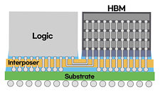
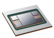
Samsung Electronics Co., Ltd., a world leader in advanced semiconductor technology, today announced the immediate availability of its next-generation 2.5D packaging technology Interposer-Cube4 (I-Cube4), leading the evolution of chip packaging technology once again. Samsung's I-CubeTM is a heterogeneous integration technology that horizontally places one or more logic dies (CPU, GPU, etc.) and several High Bandwidth Memory (HBM) dies on top of a silicon interposer, making multiple dies operate as a single chip in one package.

Samsung's new I-Cube4, which incorporates four HBMs and one logic die, was developed in March as the successor of I-Cube2. From high-performance computing (HPC) to AI, 5G, cloud and large data center applications, I-Cube4 is expected to bring another level of fast communication and power efficiency between logic and memory through heterogeneous integration.

Industry Specialists Expect Chip Shortages to Last Until 2022

Industry specialists with various analysis groups have stated that they expect the world's current chip supply shortages to not only fail to be mitigated in the first half of 2021, but that they might actually last well into 2022. It's not just a matter of existing chip supply being diverted by scalpers, miners, or other secondary-market funnels; it's a matter of fundamental lack of resources and production capacity to meet demand throughout various quadrants of the semiconductor industry. With the increased demand due to COVID-19 and the overall increasingly complex design of modern chips - and increased abundance of individual chips within the same products - foundries aren't being able to scale their capacity to meet growing demand.

As we know, the timeframe between start and finish of a given semiconductor chip can sometimes take months. And foundries have had to extend their lead times (the time between a client placing an order and that order being fulfilled) already. This happens as a way to better plan out their capacity allocation, and due to the increased complexity of installing, testing, and putting to production increasingly complex chip designs and fabrication technologies. And analysts with J.P. Morgan and Susquehanna that are in touch with the pulse of the semiconductor industry say that current demand levels are 10% to 30% higher than those that can be satisfied by the fabrication and supply subsystems for fulfilling that demand.
Return to Keyword Browsing
May 21st, 2024 13:16 EDT change timezone

New Forum Posts

Popular Reviews

Controversial News Posts