News Posts matching #production

Return to Keyword Browsing

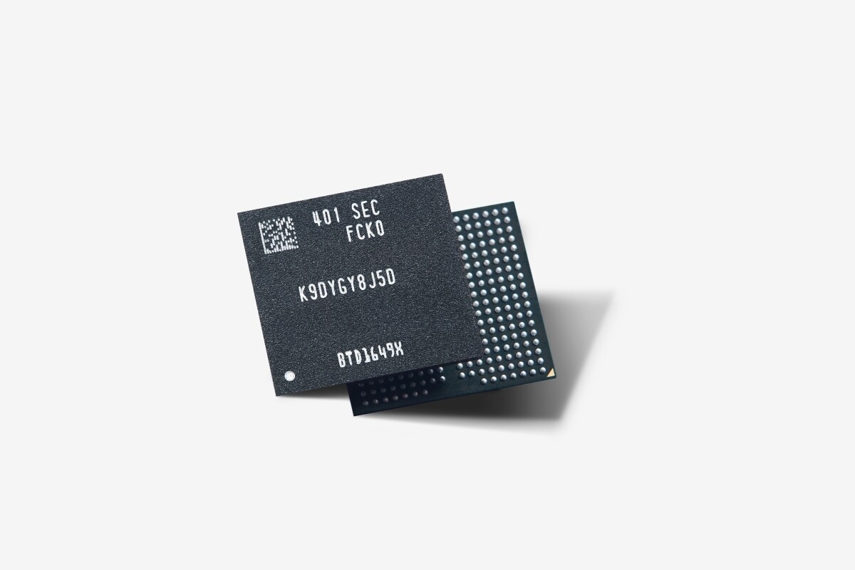
Samsung Electronics Begins Industry's First Mass Production of 9th-Gen V-NAND

Samsung Electronics Co., Ltd., the world leader in advanced memory technology, today announced that it has begun mass production for its one-terabit (Tb) triple-level cell (TLC) 9th-generation vertical NAND (V-NAND), solidifying its leadership in the NAND flash market.

"We are excited to deliver the industry's first 9th-gen V-NAND, which will bring future applications leaps forward. In order to address the evolving needs for NAND flash solutions, Samsung has pushed the boundaries in cell architecture and operational scheme for our next-generation product," said SungHoi Hur, Head of Flash Product & Technology at Samsung Electronics. "Through our latest V-NAND, Samsung will continue to set the trend for the high-performance, high-density solid state drive (SSD) market that meets the needs for the coming AI generation."

DRAM Manufacturers Gradually Resume Production, Impact on Total Q2 DRAM Output Estimated to Be Less Than 1%

Following in the wake of an earthquake that struck on April 3rd, TrendForce undertook an in-depth analysis of its effects on the DRAM industry, uncovering a sector that has shown remarkable resilience and faced minimal interruptions. Despite some damage and the necessity for inspections or disposal of wafers among suppliers, the facilities' strong earthquake preparedness of the facilities has kept the overall impact to a minimum.

Leading DRAM producers, including Micron, Nanya, PSMC, and Winbond had all returned to full operational status by April 8th. In particular, Micron's progression to cutting-edge processes—specifically the 1alpha and 1beta nm technologies—is anticipated to significantly alter the landscape of DRAM bit production. In contrast, other Taiwanese DRAM manufacturers are still working with 38 and 25 nm processes, contributing less to total output. TrendForce estimates that the earthquake's effect on DRAM production for the second quarter will be limited to a manageable 1%.

Magnitude 7.4 Earthquake in Taiwan Halts Production at TSMC and Other Foundries

At 07:58 local time, Taiwan was rocked by a magnitude 7.4 earthquake on the east coast which was felt nationwide and as far as to the southeastern parts of China and southern Japan. It caused some major damage in the east coast city of Hualien where the epicentre of the quake was located, as well as surrounding areas. The earthquake reportedly left nine people dead and over 900 people injured islandwide. TSMC, UMC, PSMC and Innolux all halted some of their production lines in the Hsinchu Science Park on the west coast of the island, although this is said to have been as a preventive step, rather than caused by actual damage from the earthquake.

All the above-mentioned companies also evacuated their staff from their factories due to the intensity of the quake, as it reached a magnitude of around four or five almost island wide. The semiconductor manufacturers are all inspecting their fabs now to make sure none of the equipment was damaged by the earthquake. Innolux also has a factory in the southern city of Kaohsiung and has reported that it has suspended production in Hsinchu, but that production in Kaohsiung wasn't affected. Local media in Taiwan hasn't made any mention of the likes of Micron or other chip manufacturers, but it's likely that the situation is similar, since all of these companies are located in the same areas on the island. Aftershocks have continued throughout the day and there's a risk for further big earthquakes to follow in the coming days.
Images courtesy of the Taiwan Central Weather Administration (CWA).

Update 15:11 UTC: Updated with an official statement from Micron below.

Researcher's Curiosity Uncovers Backdoor in Popular Linux Utility, Compromising SSH Connections

In a interesting discovery that sent a series of shockwaves through the Linux community, Andres Freund, Principal Software Engineer at Microsoft, located a malicious backdoor in the widely used compression tool called "xz Utils." The backdoor, introduced in versions 5.6.0 and 5.6.1 of the utility, can break the robust encryption provided by the Secure Shell (SSH) protocol, allowing unauthorized access to affected systems. What Andres Freund found is that the latest version of xz Utils is taking 0.5 seconds in SSH on his system, while the older system with the older version took 0.1 seconds for simple processing, prompting the user to investigate and later send a widespread act for caution. While there are no confirmed reports of the backdoored versions being incorporated into production releases of major Linux distributions, the incident has raised serious concerns among users and developers alike.

Red Hat and Debian, two of the most well-known Linux distribution developers, have reported that their recently published beta releases, including Fedora 40, Fedora Rawhide, and Debian testing, unstable, and experimental distributions, used at least one of the affected versions of xz Utils. According to Red Hat officials, the first signs of the backdoor were introduced in a February 23 update, which added obfuscated (unreadable) code to xz Utils. A subsequent update the following day introduced functions for deobfuscating the code and injecting it into code libraries during the utility's update process. The malicious code has been cleverly hidden only in the tarballs, which target upstream releases of Linux distributions.

Samsung Semiconductor Discusses "Water Stress" & Impact of Production Expansion

"The Earth is Blue," said Yuri Gagarin, the first human to journey into space. With two-thirds of its surface covered in water, Earth is a planet that exuberates its blue radiance in the dark space. However, today, the scarcity of water is a challenge that planet Earth is confronted with. For some, this may be hard to understand. What happened to our blue planet Earth? To put in numbers, more than 97% of the water on Earth consists of seawater, with another 2% locked in ice caps. That only leaves a mere 1% of water available for our daily use. The problem lies in the fact that this 1% of water is gradually becoming scarcer due to reasons such as climate change, environmental pollution, and population growth, leading to increased water stress. 'Water stress' is quantified by the proportion of water demand to the available water resources on an annual basis, indicating the severity of water scarcity as the stress index rises. Higher stress indexes signify experiencing severe water scarcity.

The semiconductor ecosystem, unsustainable without water
Because water stress issues transcend national boundaries, various stakeholders including international organizations and governments work to negotiate water resource management strategies and promote collaboration. UN designates March 22nd as an annual "World Water Day" to raise awareness about the severity of water scarcity running various campaigns. Now, it's imperative for companies to also take responsibility for the water resources given and pursue sustainable management.

China's President Believes Nation's Technological Development Unhindered, Despite Equipment Restrictions

Earlier today, Dutch Prime Minister Mark Rutte met with China's President Xi Jinping—fresh reportage has focused on their discussion of technological trade restrictions. Holland's premier had to carefully navigate the conversation around recent global tensions, most notably the prevention of fancy ASML chipmaking equipment reaching the Chinese mainland. CCTV (China's state broadcaster) selected a couple of choice quotes for inclusion in an online report—Xi remarked that: "the Chinese people also have the right to legitimate development, and no force can stop the pace of China's scientific and technological development and progress." Specific manufacturers and types of machinery were not mentioned during the meeting between state leaders, but media interpretations point to recent ASML debacles being entirely relevant, given the context of international relationships.

ASML is keen to keep Chinese firms on its order books—according to AP News: "China became ASML's second-largest market, accounting for 29% of its revenue as firms bought up equipment before the licensing requirement took effect." Revised licensing agreements have stymied the supply of ASML most advanced chipmaking tools—Chinese foundries have resorted to upgrading existing/older equipment (backed by government funding) in efforts to stay competitive with international producers. Semiconductor Manufacturing International Corporation (SMIC) is reportedly racing to get natively designed EUV machines patented (in co-operation with Huawei). Post-meeting, Rutte commented (to press) on the ongoing technology restrictions: "what I can tell you is that... when we have to take measures, that they are never aimed at one country specifically, that we always try to make sure that the impact is limited, is not impacting the supply chain, and therefore is not impacting the overall economic relationship."

InnoGrit Starts Mass Producing YRS820 PCIe 5.0 Controller, Based on RISC-V Architecture

InnoGrit's low-wattage 12 nanometer IG5666 controller popped up on the T-FORCE GE PRO PCIe 5.0 SSD series earlier in the year, but attention has turned to another consumer-grade design. Parent company—Yingren Technology—is not well known outside of China, although its InnoGrit brand has started to make inroads within Western markets. The enterprise-level YRS900 PCIe 5.0 SSD controller was announced last September—this open-source RISC-V-based solution was designed/engineered to "align with U.S. export restrictions." According to cnBeta and MyDrivers reports, a new YRS820 controller has successfully reached the mass production phase. This is a PCIe 5.0 consumer-grade controller, likely derived from its big sibling (YRS900).

According to InnoGrit presentation material, their new model is based on: "RISC-V instruction architecture, adopts a 4-channel PCIe 5.0 interface, is equipped with 8 NAND flash memory channels, supports NVMe 2.0 protocol, has an interface transmission rate of 2667MT/s, can be paired with 3D TLC/QLC, and supports a maximum capacity of up to 8 TB." Company representatives stated that the YRS820 controller is destined to be fitted on high-end consumer parts—the AI PC market segment is a key goal, since the YRS820 is able to: "accelerate data processing for specific applications and have high stability, consistency and security." cnBeta highlighted some anticipated performance figures: "YRS820 achieves sequential read 14 GB/s, sequential write 12 GB/s, random read and random write up to 2000K IOPs and 1500K IOPs respectively." InnoGrit did not reveal a release timetable, since their latest consumer-grade controller is going through a validation process. The company is currently collaborating with domestic NAND flash memory and DRAM manufacturers, as well as other industry bodies.

PlayStation VR2 Firmware Update Enables PC Access

The "iVRy VR" community-backed project has slowly chipped away at unlocking the PlayStation VR2's full potential—Sony's $550 (MSRP) virtual reality headset is locked into the PlayStation 5 ecosystem, but many gamers have requested that it become compatible with PC platforms. iVRy's progress on this front could be surpassed by first-party efforts—a month ago, Sony indicated that it was exploring new avenues: "we're pleased to share that we are currently testing the ability for PS VR2 players to access additional games on PC to offer even more game variety in addition to the PS VR2 titles available through PS5. We hope to make this support available in 2024, so stay tuned for more updates." Reports suggest that Sony's second generation product has not met sales expectations—insiders posit that company leadership has requested a pause of production. An entry into the PC market could boost the PS VR2's popularity, but it will face plenty of competition within an already "niche" segment.

iVRy has monitored Sony's progress with great interest—the former's social media account has disclosed the discovery of a new development milestone: "(their) latest firmware update enables PC access! This means it's no longer necessary to use driver/hardware workarounds to make it work on Windows. Still to be confirmed whether this update enables NVIDIA use, but all indications are that Sony's 'PC games' plans involve direct connection." The iVRy VR project has—so far—managed to (successfully) connect the PS VR2 to AMD GPU-based systems. Sony is expected to produce an official means of hooking up their headset to PCs. iVRy discussed this provision in their follow-up post: "a 'VirtualLink' adapter of some kind is still required due to PS VR2 hardware design. If Sony does intend to make 'official' PC drivers, they would need to provide this adapter to end-users."

TSMC Reportedly Investing $16 Billion into New CoWoS Facilities

TSMC is experiencing unprecedented demand from AI chip customers—unnamed parties have (fancifully) requested the construction of entirely new fabrication facilities. Taiwan's leading semiconductor contract manufacturer seems to concentrating on "sensible" expansions, mainly in the area of CoWoS packaging output—according to an Economic Daily report, company leadership and local government were negotiating over the construction of four new advanced packaging plants. Insiders propose that plans have been revised—an investment in excess of 500 billion yuan ($16 billion) will enable the founding of six new CoWoS-focused facilities. TSMC is expected to make an official announcement next month—industry moles reckon that construction work will start in April. Two (of the six total) advanced packaging plants could become fully operational before the conclusion of 2024.

Lately, TSMC has initiated an ambitious recruitment drive—targeting around 6000 new workers. A touring entity is tasked with the attraction of "talents with high enthusiasm for semiconductors." The majority of new recruits are likely heading to new or expanded Taiwan-based facilities. The Economic Daily report proposes that Chiayi City's technological hub will play host to TSMC's new CoWoS packaging plants. A DigiTimes Asia news piece (from January) posited that TSMC leadership anticipates CoWoS output reaching 44,000 units by the end of 2024. This predicted tally could grow, thanks to the (rumored) activation of additional factories. CoWoS packaging is considered to be a vital aspect of AI accelerators—insiders believe that TSMC's latest investment will boost production of NVIDIA H100 GPUs. The combined output of six new CoWoS plants will assist greatly in the creation of next-gen B100 chips.

Silicon Box Announces $3.6 Billion Foundry Deal - New Facility Marked for Northern Italy

Silicon Box, a cutting-edge, advanced panel-level packaging foundry announced its intention to collaborate with the Italian government to invest up to $3.6 billion (€3.2 billion) in Northern Italy, as the site of a new, state-of-the-art semiconductor assembly and test facility. This facility will help meet critical demand for advanced packaging capacity to enable next generation technologies that Silicon Box anticipates by 2028. The multi-year investment will replicate Silicon Box's flagship foundry in Singapore which has proven capability and capacity for the world's most advanced semiconductor packaging solutions, then expand further into 3D integration and testing. When completed, the new facility will support approximately 1,600 Silicon Box employees in Italy. The construction of the facility is also expected to create several thousand more jobs, including eventual hiring by suppliers. Design and planning for the facility will begin immediately, with construction to commence pending European Commission approval of planned financial support by the Italian State.

As well as bringing the most advanced chiplet integration, packaging, and testing to Italy, Silicon Box's manufacturing process is based on panel-level-production; a world leading, first-of-its-kind combination that is already shipping product to customers from its Singapore foundry. Through the investment, Silicon Box has plans for greater innovation and expansion in Europe, and globally. The new integrated production facility is expected to serve as a catalyst for broader ecosystem investments and innovation in Italy, as well as the rest of the European Union.

US Government to Announce Massive Grant for Intel's Arizona Facility

According to the latest report by Reuters, the US government is preparing to announce a multi-billion dollar grant for Intel's chip manufacturing operations in Arizona next week, possibly worth more than $10 billion. US President Joe Biden and Commerce Secretary Gina Raimondo will make the announcement, which is part of the 2022 CHIPS and Science Act aimed at expanding US chip production and reducing dependence on China and Taiwan manufacturing. The exact amount of the grant has yet to be confirmed, but rumors suggest it could exceed $10 billion, making it the most significant award yet under the CHIPS Act. The funding will include grants and loans to bolster Intel's competitive position and support the company's US semiconductor manufacturing expansion plans. This comes as a surprise just a day after the Pentagon reportedly refused to invest $2.5 billion in Intel as a part of a secret defense grant.

Intel has been investing significantly in its US expansion, recently opening a $3.5 billion advanced packaging facility in New Mexico, supposed to create extravagant packaging technology like Foveros and EMIB. The chipmaker is also expanding its semiconductor manufacturing capacity in Arizona, with plans to build new fabs in the state. Arizona is quickly becoming a significant hub for semiconductor manufacturing in the United States. In addition to Intel's expansion, Taiwan Semiconductor Manufacturing Company (TSMC) is also building new fabs in the state, attracting supply partners to the region. CHIPS Act has a total funding capacity of $39 billion allocated for semiconductor production and $11 billion for research and development. The Intel grant will likely cover the production part, as Team Blue has been reshaping its business units with the Intel Product and Intel Foundry segments.

Malaysian Government Targeting Front-end Semiconductor Manufacturing

Global tensions have caused big semiconductor manufacturers to consider a diversification of production facilities outside of China—most news headlines have concentrated on new operations or advancement/upgrades in the USA, India and Japan. As reported by the Financial Times, Malaysia has quietly established itself as a haven for big chip firms—a "free-trade zone" on the island of Penang is home to fancy Intel and Micron production operations. Team Blue's emerging next-gen Battlemage GPU was spotted during a summer 2023 press event—at the time, HardwareLuxx reported the existence of a "BMG G10" die in Intel Malaysia's Failure Lab. Micron celebrated its 45th anniversary last October, with the opening of a new cutting-edge assembly and test facility in Batu Kawan, Penang. The two firms—and a few others—established roots in Malaysia decades ago, but future investments are set to boost the nation's semiconductor industry.

According to Tom's Hardware: "Intel will spend a whopping $7 billion on new, Malaysian chip assembly and testing facilities. The overall total of foreign Malaysian investment in 2023 was $12.8 billion, and that exceeded its seven-year combined total from 2013 to 2020." Anwar Ibrahim, the country's Prime Minister, is keen to see manufacturing advance to a higher-value tier—a February FT.com interview reveals that this is a "critical goal" for his administration. The establishment of a front-end semiconductor manufacturing plant would be welcomed the most—Zafrul Aziz, Trade Minister of Malaysia, stated (to FT): "I am optimistic we will attract more than one. All it takes is one to kick-start a wave." Historically, Malaysian facilities have been created to deal with the back end of semiconductor supply chains—e.g. packing, assembling and testing components. Company leaderships consider these activities to be of lower value, due to their less complex nature. Certain foreign investments, into Malaysian plants, have come from Chinese firms—a growing presence of PRC-owned plants could complicate matters. The Financial Times article presents a possible future scenario, with the US Government stepping in...if alarmed to a certain degree.

Samsung Accelerates R&D of Glass Substrate Chip Packaging

The Samsung Group has formed a new cross-department alliance—according to South Korea's Sedaily—this joint operation will concentrate on the research and development of a "dream substrate." The company's Electronics, Electrical Engineering, and Display divisions are collaborating in order to accelerate commercialization of "glass substrate" chip packaging. Last September, Intel revealed its intention to become an industry leader in "glass substrate production for next-generation advanced packaging." Team Blue's shiny new Arizona fabrication site will be taking on this challenge, following ten years of internal R&D work. Industry watchdogs reckon that mass production—in North America—is not expected to kick off anytime soon. Sensible guesstimates suggest a start date somewhere in 2030.

The Sedaily article states that Samsung's triple department alliance will target "commercialization faster than Intel." Company representatives—in attendance at CES 2024—set a 2026 window as their commencement goal for advanced glass substrate chip package mass production. An unnamed South Korean industry watcher has welcomed a new entrant on the field: "as each company possesses the world's best technology, synergies will be maximized in glass substrate research, which is a promising field...it is also important to watch how the glass substrate ecosystem of Samsung's joint venture will be established." Glass substrate packaging is ideal for "large-area and high-performance chip combinations" due to inherent heat-resistant properties and material strength. So far, the semiconductor industry has struggled with its development—hence the continued reliance on plastic boards and organic materials.

Global Top 10 Foundries Q4 Revenue Up 7.9%, Annual Total Hits US$111.54 Billion in 2023

The latest TrendForce report reveals a notable 7.9% jump in 4Q23 revenue for the world's top ten semiconductor foundries, reaching $30.49 billion. This growth is primarily driven by sustained demand for smartphone components, such as mid and low-end smartphone APs and peripheral PMICs. The launch season for Apple's latest devices also significantly contributed, fueling shipments for the A17 chipset and associated peripheral ICs, including OLED DDIs, CIS, and PMICs. TSMC's premium 3 nm process notably enhanced its revenue contribution, pushing its global market share past the 60% threshold this quarter.

TrendForce remarks that 2023 was a challenging year for foundries, marked by high inventory levels across the supply chain, a weak global economy, and a slow recovery in the Chinese market. These factors led to a downward cycle in the industry, with the top ten foundries experiencing a 13.6% annual drop as revenue reached just $111.54 billion. Nevertheless, 2024 promises a brighter outlook, with AI-driven demand expected to boost annual revenue by 12% to $125.24 billion. TSMC, benefiting from steady advanced process orders, is poised to far exceed the industry average in growth.

SMIC Prepares for 3 nm Node Development, Requires Chinese Government Subsidies

SMIC, China's largest semiconductor manufacturer, is reportedly assembling a dedicated team to develop 3 nm semiconductor node technology, following reports of the company setting up 5 nm chip production for Huawei later this year. This move is part of SMIC's efforts to achieve independence from foreign companies and reduce its reliance on US technology. According to a report from Joongang, SMIC's initial goal is to commence operations of its 5 nm production line, which will mass-produce Huawei chipsets for various products, including AI silicon. However, SMIC is already looking beyond the 5 nm node. The company has assembled an internal research and development team to begin work on the next-generation 3 nm node.

The Chinese manufacturer is expected to accomplish this using existing DUV machinery, as ASML, the sole supplier of advanced EUV technology, is prohibited from providing equipment to Chinese companies due to US restrictions. It is reported that one of the biggest challenges facing SMIC is the potential for low yields and high production costs. The company is seeking substantial subsidies from the Chinese government to overcome these obstacles. Receiving government subsidies will be crucial for SMIC, especially considering that its 5 nm chips are expected to be up to 50 percent more expensive than TSMC's due to the use of older DUV equipment. The first 3 nm wafers from SMIC are not expected to roll out for several years, as the company will prioritize the commercialization of Huawei's 5 nm chips. This ambitious undertaking by SMIC represents a significant challenge for the company as it strives to reduce its dependence on foreign semiconductor technology and establish itself as an essential player in the global manufacturing industry.

Frogware's "The Sinking City 2" Has Evolved into a Full-Blown Horror Game

The characters in a Lovecraft story are susceptible to… mutation. Minds and bodies are forever altered by exposure to the horrors hiding in the darker corners of the world. It's perhaps no surprise, then, that The Sinking City 2—which just got a world premiere in the latest Xbox Partner Preview broadcast—has undergone its own unexpected change. Where the first game was a detective adventure, with horror bubbling up from its flooded world, its sequel has taken on a darker, more aggressive form. The Sinking City 2 is a true horror game now, with more emphasis on combat, while keeping a Lovecraftian narrative close to its twisted heart.

"The Sinking City is one of our most successful titles, because of our stronger horror genre leanings and the setting," Frogwares Head of Publishing, Sergey Oganesyan tells me. "For us, it was kind of a breakthrough, and we are super excited to work on a full-scale horror game. We have created quite a few detective adventures in the past, so now we're going to mix things up to keep doing what people love from us - meaning story-rich experiences - while still being able to evolve."

Drop Discusses Driver Geometry on Axel Grell's OAE1 Signature Headphones

Everyone perceives sound differently. Your ear is not like a measuring microphone. Because of this, it's important to understand how sound is perceived and what factors influence that perception. In creating the OAE1 signature with Axel Grell, we studied how sound is perceived. This premise drove the unique geometry and driver placement for the OAE1 Signature headphones. Since our ears, with all their unique characteristics, act as a natural equalizer to all that we hear, it makes sense that headphones should do more to use the structure of the pinna to guide soundwaves into the ear canal.

To achieve this effect, the transducers are placed much further forward and angled back towards the ear. By positioning the transducer further out and away it enables the soundwaves to fully encompass the pinna (the external part of the ear), allowing for an increase in spectral information and a more natural sound field for the listener. By contrast, the majority of headphones on the market are much closer to the ear and positioned perpendicular to the opening of the canal which bypasses much of the pinna's structure (and therefore the natural sound-shaping function of the ear itself).

Intel Reportedly Close to Receiving $3.5 Billion Investment for US Military Chip Solutions

The US government is reported to be preparing a very healthy $3.5 billion investment in Intel Corporation—a mid-week published Bloomberg article proposes that the White House has authored a new "fast-moving spending bill." Congressional aides believe that Team Blue—upon official approval/signing off of funds—will be tasked with the production of advanced semiconductors for military and intelligence programs. Bloomberg posits that the resources will be sourced from a "Secure Enclave" project, seemingly linking to a wider tranche of funds within the US government's CHIPS and Science Act. The agreement/contract is expected to run over a period of three years. According to Bloomberg: "the Senate is expected to pass the legislation by a Saturday (March 9) deadline."

Reports from last November suggested that Intel leadership and US government representatives had engaged in negotiations regarding funds for military and intelligence chip applications—the construction costs for new manufacturing facilities were estimated to be in the $3 billion to $4 billion range. A Commerce Department statement was submitted to Bloomberg, but they only commented on an overall $10 billion budget: "We are still reviewing the effect of the appropriations text on the program...(we look) forward to continuing to work with Congress on implementing the Chips and Science Act in a manner the promotes our economic and national security." TSMC, Micron and Samsung are expected to receive "multi-billion-dollar awards" in the near future—these multinational corporations will assist in a bolstering of North American chip manufacturing capabilities.

NVIDIA Reportedly Sampling SK Hynix 12-layer HBM3E

South Korean tech insiders believe that SK Hynix has sent "12-layer DRAM stacked HBM3E (5th generation HBM)" prototype samples to NVIDIA—according a ZDNET.co.kr article, initial examples were shipped out last month. Reports from mid-2023 suggested that Team Green had sampled 8-layer HBM3E (4th gen) units around summer time—with SK Hynix receiving approval notices soon after. Another South Korean media outlet, DealSite, reckons that NVIDIA's memory qualification process has exposed HBM yield problems across a number of manufacturers. SK Hynix, Samsung and Micron are competing fiercely on the HBM3E front—with hopes of getting their respective products attached to NVIDIA's H200 AI GPU. DigiTimes Asia proposed that SK Hynix is ready to "commence mass production of fifth-generation HBM3E" at some point this month.

SK Hynix is believed to be leading the pack—insiders believe that yield rates are good enough to pass early NVIDIA certification, and advanced 12-layer samples are expected to be approved in the near future. ZDNET reckons that SK Hynix's forward momentum has placed it an advantageous position: "(They) supplied 8-layer HBM3E samples in the second half of last year and passed recent testing. Although the official schedule has not been revealed, mass production is expected to begin as early as this month. Furthermore, SK Hynix supplied 12-layer HBM3E samples to NVIDIA last month. This sample is an extremely early version and is mainly used to establish standards and characteristics of new products. SK Hynix calls it UTV (Universal Test Vehicle)... Since Hynix has already completed the performance verification of the 8-layer HBM3E, it is expected that the 12-layer HBM3E test will not take much time." SK Hynix's Vice President recently revealed that his company's 2024 HBM production volumes for were already sold out, and leadership is already preparing innovations for 2025 and beyond.

IBM Intros AI-enhanced Data Resilience Solution - a Cyberattack Countermeasure

Cyberattacks are an existential risk, with 89% of organizations ranking ransomware as one of the top five threats to their viability, according to a November 2023 report from TechTarget's Enterprise Strategy Group, a leading analyst firm. And this is just one of many risks to corporate data—insider threats, data exfiltration, hardware failures, and natural disasters also pose significant danger. Moreover, as the just-released 2024 IBM X-Force Threat Intelligence Index states, as the generative AI market becomes more established, it could trigger the maturity of AI as an attack surface, mobilizing even further investment in new tools from cybercriminals. The report notes that enterprises should also recognize that their existing underlying infrastructure is a gateway to their AI models that doesn't require novel tactics from attackers to target.

To help clients counter these threats with earlier and more accurate detection, we're announcing new AI-enhanced versions of the IBM FlashCore Module technology available inside new IBM Storage FlashSystem products and a new version of IBM Storage Defender software to help organizations improve their ability to detect and respond to ransomware and other cyberattacks that threaten their data. The newly available fourth generation of FlashCore Module (FCM) technology enables artificial intelligence capabilities within the IBM Storage FlashSystem family. FCM works with Storage Defender to provide end-to-end data resilience across primary and secondary workloads with AI-powered sensors designed for earlier notification of cyber threats to help enterprises recover faster.

TSMC Arizona Celebrates "Topping Out" Milestone at Second Fab Site

TSMC Arizona's second semiconductor fabrication site has celebrated a "topping out" milestone—as documented in an official blog post (via LinkedIn) from yesterday. Workers were photographed installing an important/final piece of structure—the aforementioned "topping out" milestone signifies: "the last steel beam being raised into place on a construction project." The Taiwanese multinational semiconductor contract manufacturer has had a rough time in establishing operations out in the desert/greater Phoenix area—the "Fab 21 Phase 2" plant is not expected to meet its original 2026 opening window. TSMC Chairman Mark Liu is reportedly leaving his position due to consistent Arizona-related problems and delays.

The TSMC LinkedIn account shared some additional and certainly much-needed positive news: "We also recently achieved the topping milestone on our second fab's auxiliary buildings, which will supply the necessary utilities infrastructure to the second fab clean room." Thursday's blog (February 22) also discloses that the primary site—Fab 21 Phase 1—is still on track to begin production within the first half of 2025, thanks to "significant" bursts in construction progress. The author moved onto future production prospects: "Once operational, our two fabs at TSMC Arizona will manufacture the most advanced semiconductor technology in the U.S., creating 4,500 direct high-tech, high-wage jobs and enabling our customers' leadership in the high-performance computing and artificial intelligence era for decades."

SK Hynix VP Reveals HBM Production Volumes for 2024 are Sold Out

SK Hynix Vice President Kitae Kim presides over the company's HBM Sales & Marketing (S&M) department—an official leadership blog profile reveals that the executive played a key role in making the South Korean supplier's high bandwidth memory (HBM) product line "a superstar of the semiconductor memory industry in 2023." Growing demand for powerful AI processors has placed SK Hynix in a more comfortable position, following recessive spells—including a major sales downturn in 2022. NVIDIA is the market leader in AI processing chips, and many of its flagship enterprise designs are fitted with cutting-edge SK Hynix memory modules. Kim noted that his firm has many notable international clients: "HBM is a revolutionary product which has challenged the notion that semiconductor memory is only one part of an overall system...in particular, SK Hynix's HBM has outstanding competitiveness. Our advanced technology is highly sought after by global tech companies."

The VP outlined how artificial intelligence industries are fuelling innovations: "With the diversification and advancement of generative AI services, demand for HBM, an AI memory solution, has also exploded. HBM, with its high-performance and high-capacity characteristics, is a monumental product that shakes the conventional wisdom that memory semiconductors are only a part of the overall system. In particular, SK Hynix HBM's competitiveness is outstanding." Business is booming, so much so that nothing can be added to this year's HBM order books: "Proactively securing customer purchase volumes and negotiating more favorable conditions for our high-quality products are the basics of semiconductor sales operations. With excellent products in hand, it's a matter of speed. Our planned production volume of HBM this year has already sold out. Although 2024 has just begun, we've already started preparing for 2025 to stay ahead of the market."

US Commerce Chief: Nation Requires Additional Chip Funding

US Commerce Secretary, Gina Raimondo, was a notable guest speaker during yesterday's Intel Foundry Direct Connect Keynote—she was invited on (via a video link) to discuss the matter of strengthening the nation's semiconductor industry, and staying competitive with global rivals. During discussions, Pat Gelsinger (Intel CEO) cheekily asked whether a "CHIPS Act Part Two" was in the pipeline. Raimondo responded by stating that she is till busy with the original $52 billion tranche: "I'm out of breath running as fast as I can implementing CHIPS One." Earlier this week, her department revealed a $1.5 billion planned direct fund for GlobalFoundries: "this investment will enable GF to expand and create new manufacturing capacity and capabilities to securely produce more essential chips for automotive, IoT, aerospace, defense, and other vital markets."

Intel is set to receive a large grant courtesy of the US government's 2022-launched CHIPS and Science Act—exact figures have not been revealed to the public, but a Nikkei Asia report suggests that Team Blue will be benefiting significantly in the near future: "While the Commerce Department has not yet announced how much of the funding package's $52 billion it would grant Intel, the American chipmaker is expected to get a significant portion, according to analysts and officials close to the situation." Raimondo stated that: "Intel is an American champion company and has a very huge role to play in this revitalization." The US Commerce Chief also revealed that she had spoken with artificial intelligence industry leaders, including OpenAI's Sam Altman, about the ever-growing demand for AI-crunching processors/accelerators/GPUs. The country's semiconductor production efforts could be bolstered once more, in order to preserve a competitive edge—Raimondo addressed Gelsinger's jokey request for another batch of subsidies: "I suspect there will have to be—whether you call it Chips Two or something else—continued investment if we want to lead the world...We fell pretty far. We took our eye off the ball."

OpenAI Potentially Seeking $5-7 Trillion Investment in Establishment of Fab Network

Various news outlets have been keeping tabs on OpenAI's CEO—Sam Altman—the AI technology evangelist was reported to be pursuing an ambitious proprietary AI chip project in early 2024. Inside sources pointed to late-January negotiations with important investment personnel in the Middle East—many believe that OpenAI leadership is exploring the idea of establishing its own network of semiconductor production plants. Late last week, The Wall Street Journal followed up on last month's AI industry rumors: "(Altman) has another great ambition: raising trillions of dollars to reshape the global semiconductor industry. The OpenAI chief executive officer is in talks with investors including the United Arab Emirates government to raise funds for a wildly ambitious tech initiative that would boost the world's chip-building capacity, expand its ability to power AI." One anonymous insider reckons that "the project could require raising as much as $5 trillion to $7 trillion."

TSMC is reportedly in the equation—Altman allegedly conducted talks with top brass last month—their expertise in cutting edge fabrication techniques would be of great value, although it is somewhat futile to reveal too many industry secrets given the sheer scale of OpenAI's (reported) aggressive expansion plans. The Wall Street Journal (WSJ) suggests that the embryonic venture is far more "open" than previously reported—a collaborative venture could be established once funding is secured, although Altman & Co. face "significant obstacles" en route. WSJ proposes that the somewhat OpenAI-centric fabrication network is best founded by a joint partnership—involving multiple investors, contract chip manufacturers (perhaps TSMC), and energy/power providers. OpenAI appears to be the "primary buyer" of resultant fabricated AI chips, with manufacturing services also offered to other clients. The scale of such an endeavor is put into perspective by WSJ's analysis (via inside sources): "Such a sum of investment would dwarf the current size of the global semiconductor industry. Global sales of chips were $527 billion last year and are expected to rise to $1 trillion annually by 2030. Global sales of semiconductor manufacturing equipment—the costly machinery needed to run chip factories—last year were $100 billion, according to an estimate by the industry group SEMI."

Ubisoft Roadmaps "Skull and Bones" Seasonal Content

Skull and Bones sets sail on February 16, welcoming players to the cutthroat world of the Indian Ocean during the Golden Age of Piracy. While you start off as a shipwrecked outcast, you'll fight, forge alliances, and make enemies as you build your empire and become a kingpin of the seas. And the adventure doesn't stop once you've reached the top. As a kingpin, you'll have the power to take on difficult endgame events and challenges to earn more riches and unlock new items, but that's just the start. Skull and Bones' first year will bring four seasons of new enemies to the Indian Ocean, starting with a pestilent pirate lord who rains poison from the sky.

In a recent co-op gameplay session, we had the opportunity to play around in Skull and Bones' endgame. Playing at the Kingpin level, the highest Infamy ranking, we had a fleet of ships and an arsenal of weapons at our disposal to plunder outposts and seize their means of production, hunt down a devastating sea monster, and sail into battle against the aforementioned pirate lord. Skull and Bones endgame is full of opportunities to take on legendary challenges, cement yourself as a powerhouse in different regions of the Indian Ocean, and even change up a few game mechanics.
Return to Keyword Browsing
Apr 30th, 2024 22:33 EDT change timezone

New Forum Posts

Popular Reviews

Controversial News Posts