News Posts matching #semiconductor manufacturing

Return to Keyword Browsing

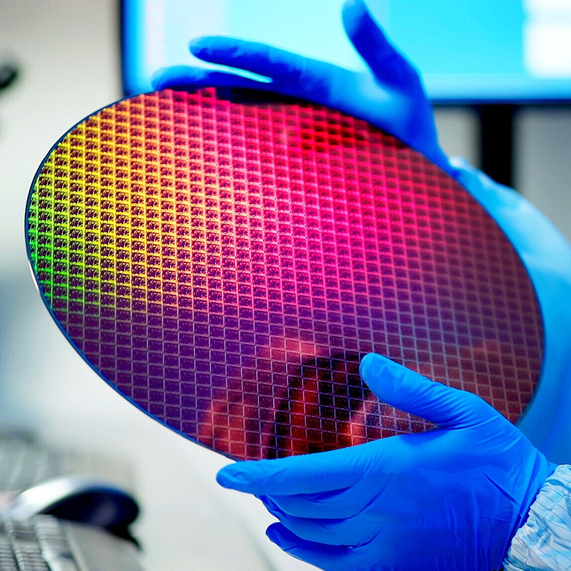
China Approves Licences for Rare Metal Exports

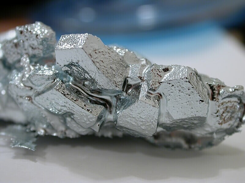
The Chinese government introduced restrictions on the export of gallium and germanium (plus their chemical compounds)—both crucial materials in the computer chip manufacturing process—a couple of months ago. Big players within the semiconductor industry shrugged this off as a minor inconvenience, and simply shifted to more expensive sources. Prior to an August 1 implementation of new rulings, according to Reuters, China exported 36.48 metric tons of germanium, and 22.72 tons of gallium (starting January 2023). Customers were in a rush to acquire as much material as possible, before the "cut off" date—so 8.63 tons of germanium and 5.15 tons of gallium got shifted overseas throughout July.

Reuters has kept a watchful eye on the situation since then—its latest report states that "China's exports of germanium and gallium items plunged in August, the first month of the export controls, customs data showed on Wednesday (September 20)." A Ministry of Commerce spokesman, He Yadong, last week revealed that his department will be granting a limited number of export licenses to interested parties, on the condition that these local companies "meet relevant requirements." An undisclosed percentage of submitted applications have already received government approval. Signed paperwork reportedly gives the thumbs up to "dual use" purposes, implying that potential customers are in the military and civilian fields.

TSMC Could Delay 2 nm Mass Production to 2026

According to TechNews.tw, TSMC could postpone its 2 nm semiconductor manufacturing node for 2026. If the rumors about TSMC's delayed 2 nm production schedule are accurate, the implications could reverberate throughout the semiconductor industry. TSMC's alleged hesitancy could be driven by multiple factors, including the architectural shift from FinFET to Gate-All-Around (GAA) and potential challenges related to scaling down to 2 nm. The company is a crucial player in this space, and a delay could offer opportunities for competitors like Samsung, which has already transitioned to GAA transistor architecture for its 3 nm chips. Given the massive demand for advanced nodes due to the rise of AI, IoT, and other next-gen technologies, it is surprising to hear "sluggish" demand reports.

However, it's also possible that it's too early for customers to make firm commitments for 2025 and beyond. TSMC has dismissed these rumors, stating that construction is progressing according to plan, which includes having 2 nm pilot run in 2024, and mass production in the second half of 2025.. Despite this, any delay in TSMC's roadmap could serve as a catalyst for shifts in market dynamics. Companies that rely heavily on TSMC's advanced nodes might need to reassess their timelines and strategies. Moreover, if Samsung can capitalize on this opportunity, it could somewhat level the playing field. As of now, though, it's essential to approach these rumors with caution until more concrete information becomes available.

ITRI Leads Global Semiconductor Collaboration for Heterogeneous Integration to Pioneer Pilot Production Solutions

The introduction of Generative AI (GAI) has significantly increased the demand for advanced semiconductor chips, drawing increased attention to the development of complex calculations for large-scale AI models and high-speed transmission interfaces. To assist the industry in grasping the key to high-end semiconductor manufacturing and integration capabilities, the Heterogeneous Integrated Chiplet System Package (Hi-CHIP) Alliance brings together leading semiconductor companies from Taiwan and around the world to provide comprehensive services, spanning from packaging design, testing and verification, to pilot production. Since its establishment in 2021, the alliance has accumulated important industry players as its members, including EVG, Kulicke and Soffa (K&S), USI, Raytek Semiconductor, Unimicron, DuPont, and Brewer Science. Looking forward, the alliance is set to actively explore its global market potential.

Dr. Shih-Chieh Chang, General Director of Electronic and Optoelectronic System Research Laboratories at ITRI and Chairman of the Hi-CHIP Alliance, indicated that advanced manufacturing processes have led to a considerable increase in IC design cycles and costs. Multi-dimensional chip design and heterogeneous integrated packaging architecture are key tools to tackle this demand in semiconductors. On top of that, the advent of GAI such as ChatGPT, which demands substantial computing power and transmission speed, requires even higher levels of integration capacity in chip manufacturing. ITRI has been committed to developing manufacturing technologies and upgrading materials and equipment to enhance heterogeneous integration technologies. Achievements include the fan-out wafer level packaging (FOWLP), 2.5 and 3D chips, embedded interposer connections (EIC), and programmable packages. With both local and foreign semiconductor manufacturer members, the Hi-CHIP Alliance is establishing an advanced packaging process production line to provide an integrated one-stop service platform.

China Ramps Up Semiconductor Imports Ahead of Export Restrictions

China has sharply increased imports of semiconductor manufacturing equipment in recent months, customs data reveals. The country's purchases of chip production tools surged to record highs of nearly $5 billion in June and July, a 70% increase versus the same period last year, which amounted to $2.9 billion. The spike comes right before export restrictions on advanced chipmaking equipment are implemented by the U.S. and its allies. The moves aim to slow China's technological advancement, but Chinese chipmakers are stockpiling to avoid disruptions. Much of the equipment comes from the Netherlands and Japan, which have imposed licensing requirements on certain tool exports. While it's unclear how many are affected, the rush suggests China wants to expand production capacity and buffer against supply chain issues.

Chinese firms like SMIC and YMTC rely heavily on U.S., Dutch, and Japanese suppliers for cutting-edge manufacturing equipment. They are utilizing imported tools to boost the output of mature chips not subject to controls, particularly for electric vehicles, renewable energy, and industrial applications. Significantly, imports from the Netherlands doubled as lithography machines were delivered to Chinese foundries. Purchases from Japan also rose as companies procured etching tools and wafer coaters after 2020 U.S. restrictions. Newly established foundries backed by local governments contributed as Beijing pushed chip production expansions. Despite export control challenges, China aims to keep advancing its semiconductor capabilities. The import spike highlights intensified efforts to build self-sufficiency using older technology not covered by current limits.

Global Semiconductor Industry on Track for 2024 Recovery but Near-Term Headwinds Remain

With sequential IC sales declines beginning to moderate, the global semiconductor industry appears to be nearing the end of a downcycle and is expected to begin to recover in 2024, SEMI, in partnership with TechInsights, reported in the Semiconductor Manufacturing Monitor. In Q3 2023, electronics sales are projected to post healthy quarter-on-quarter growth of 10%, while memory IC sales are expected to log double-digit growth for the first time since the downturn started in Q3 2022. Logic IC sales are predicted to remain stable and improve as demand gradually recovers.

Headwinds will continue for the semiconductor manufacturing sector in the second half of the year, SEMI and TechInsights reported. Drawdowns of high inventory at integrated device manufacturer (IDM) and fabless companies will continue to suppress fab utilization rates to much lower levels than those in the first half of 2023. The weakness is projected to extend declines in capital equipment billings and silicon shipments for the rest of the year despite stable results in the first half of 2023.

TSMC is Building a $10B Fab In Germany

TSMC (TWSE: 2330, NYSE: TSM), Robert Bosch GmbH, Infineon Technologies AG (FSE: IFX / OTCQX: IFNNY), and NXP Semiconductors N.V. (NASDAQ: NXPI) today announced a plan to jointly invest in European Semiconductor Manufacturing Company (ESMC) GmbH, in Dresden, Germany to provide advanced semiconductor manufacturing services. ESMC marks a significant step towards construction of a 300 mm fab to support the future capacity needs of the fast-growing automotive and industrial sectors, with the final investment decision pending confirmation of the level of public funding for this project. The project is planned under the framework of the European Chips Act.

The planned fab is expected to have a monthly production capacity of 40,000 300 mm (12-inch) wafers on TSMC's 28/22 nanometer planar CMOS and 16/12 nanometer FinFET process technology, further strengthening Europe's semiconductor manufacturing ecosystem with advanced FinFET transistor technology and creating about 2,000 direct high-tech professional jobs. ESMC aims to begin construction of the fab in the second half of 2024 with production targeted to begin by the end of 2027.

Major Foundries Not Too Concerned About China's Restrictions on Rare Metal Exports

China announced on Monday (June 3) that it would restrict exports of two rare metals——both crucial materials in the computer chip manufacturing process. The nation's Ministry of Commerce stated that their new measures were necessary to "safeguard national security and interests". The Chinese government is contending with several sanctions from Western countries—most notably their access to advanced semiconductor manufacturing equipment is now heavily controlled. Reuters has contacted a number of foundries about the potential impact of rare material shipment limitations. Taiwan Semiconductor Manufacturing Company (TSMC) has shrugged it off as a minor inconvenience, their spokesperson stated: "After evaluation, we do not expect the export restrictions on raw materials gallium and germanium will have any direct impact on TSMC's production. We will continue to monitor the situation closely."

WIN Semiconductors Corp—a Taiwanese firm that specializes in the provision of gallium arsenide wafers—informed the news agency about its low-level reliance on Chinese mineral sources. They are able to sidestep and procure gallium and germanium from suppliers located in Germany, Japan, and North America. The Japanese Semiconductor Equipment Association stated that it was too early to tell whether China's export restrictions will result in material shortages. Supply chains could be disrupted to some degree due to China controlling over 90% of the world's gallium and germanium production, but DigiTimes Asia proposes that new sanctions will not prohibit production and export activities. According to experts in the field supply lines will continue to operate, with buyers required to jump through some extra hoops in order to gain approval for certain market segments. The purification of gallium and germanium is mostly controlled by American and Japanese entities—the processed form of these metals is used in semiconductor production—DigiTimes reckons that these firms will probably feel the initial impact of new trade restrictions.

Despite Export Ban on Equipment, China's Semiconductor Expansion in Mature Processes Remains Strong

On June 30th, the Netherlands introduced new export restrictions on advanced semiconductor manufacturing equipment. Despite facing export controls from the US, Japan, and the Netherlands, TrendForce anticipates the market share of Chinese foundries in terms of 12-inch wafer production capacity will likely increase from 24% in 2022 to an estimated 26% in 2026. Moreover, if the exports of 40/28 nm equipment eventually receive approval, there's a chance that this market share could expand even further, possibly reaching 28% by 2026. This growth potential should not be dismissed.

Several manufacturing processes including photolithography, deposition, and epitaxy will be subject to these recent export restrictions. Beginning September 1st, the export of all controlled items will require formal authorization. TrendForce reports that Chinese foundries have been primarily developing mature processes like 55 nm, 40 nm, and 28 nm. Furthermore, demand for deposition equipment can be largely met by local Chinese vendors, meaning concerns regarding expansion and development are minimal. The main limiting factor, however, remains the equipment used in photolithography.

Metalenz Launches Its Metasurface Optics on the Open Market in Partnership With UMC

Metalenz, the world leader in metasurface optics, today announced it has partnered with leading semiconductor foundry United Microelectronics Corporation ("UMC") to release its direct supply chain to mass production and bring the unrivaled scale and precision of semiconductor manufacturing to the optics industry. The announcement marks the launch of metasurface optics on the open market for the first time and follows multiple design wins for Metalenz with leading OEMs in Asia.

"After initially designing meta-optics in partnership with one of the leading suppliers of 3D sensing solutions, we are now engaged with OEMs directly to bring the benefits of metasurface optics to their 3D sensing applications. By partnering with a world-class foundry like UMC, we gain the manufacturing capabilities, expertise, and global reach to serve customers interested in adopting our meta-optics technology," said Rob Devlin, Co-founder and CEO of Metalenz. "This will further accelerate our growth as we are becoming the leading provider of precision optics for 3D sensing solutions."

U.S. Administration Outlines Plan to Strengthen Semiconductor Supply Chains

Today, the U.S. Department of Commerce shared the Biden-Harris Administration's strategic vision to strengthen the semiconductor supply chain through CHIPS for America investments. To advance this vision, the Department announced a funding opportunity and application process for large semiconductor supply chain projects and will release later in the fall a separate process for smaller projects. Large semiconductor supply chain projects include materials and manufacturing equipment facility projects with capital investments equal to or exceeding $300 million, and smaller projects are below that threshold.

The announcement leads into the Biden-Harris Administration's Investing in America tour, where Secretary Raimondo and leaders in the Administration will fan across more than 20 states to highlight investments, jobs, and economic opportunity driven by President Biden's Investing in America agenda and the historic legislation he's passed in his first two years in office, including the bipartisan CHIPS and Science Act.

Lam Research Introduces World's First Bevel Deposition Solution to Increase Yield in Chip Production

Lam Research Corp. (Nasdaq: LRCX) today introduced Coronus DX, the industry's first bevel deposition solution optimized to address key manufacturing challenges in next-generation logic, 3D NAND and advanced packaging applications. As semiconductors continue to scale, manufacturing becomes increasingly complex with hundreds of process steps needed to build nanometer-sized devices on a silicon wafer. In a single step, Coronus DX deposits a proprietary layer of protective film on both sides of the wafer edge that helps prevent defects and damage that can often occur during advanced semiconductor manufacturing. This powerful protection increases yield and enables chipmakers to implement new leading-edge processes for the production of next-generation chips. Coronus DX is the newest addition to the Coronus product family and extends Lam's leadership in bevel technology.

"In the era of 3D chipmaking, production is complex and costly," said Sesha Varadarajan, senior vice present of the Global Products Group at Lam Research. "Building on Lam's expertise in bevel innovation, Coronus DX helps drive more predictable manufacturing and significantly higher yield, paving the way for adoption of advanced logic, packaging and 3D NAND production processes that weren't previously feasible."

Intel, German Government Agree on Increased Scope for Wafer Fabrication Site in Magdeburg

Intel and the German federal government have signed a revised letter of intent for Intel's planned leading-edge wafer fabrication site in Magdeburg, the capital of Saxony-Anhalt state in Germany. The agreement encompasses Intel's expanded investment in the site, now expected to be more than 30 billion euros for two first-of-a-kind semiconductor facilities (also known as "fabs") in Europe, along with increased government support that includes incentives, reflecting the expanded scope and change in economic conditions since the site was first announced.

Intel acquired the land for the project in November 2022, and the first facility is expected to enter production in four to five years following the European Commission's approval of the incentive package. Given the current timeline and scale of the investment, Intel plans to deploy more advanced Angstrom-era technology in the facilities than originally envisioned. The Magdeburg site will serve Intel products and Intel Foundry Services customers.

Intel to Get 9.9 Billion Euros in State Subsidies for German Facility

Intel has been planning to build its next-generation semiconductor manufacturing plant in Germany for a long time. Today, we have more information thanks to the Handelsblatt business and financial newspaper. According to the Handelsblatt, Intel is in talks with the German government to get as much as 9.9 billion Euros in state subsidies, a target price much higher than the previously agreed 6.8 billion Euros. Federal Economics Minister Robert Habeck has been reportedly working intensively to get the amount of state aid for Intel to be this high. Intel's CEO Patrick Gelsinger is supposed to seal the deal on Monday when he will sign the agreement in the Chancellery.

As reported, the location of the next-generation facility will be Saxony-Anhalt, with the more precise location to be known on Monday. Also, we expect to hear what manufacturing node will the upcoming facility produce at the beginning.

EU Approves €8 Billion Fund to Aid Semiconductor Research

According to the report coming from Bloomberg, European Union has approved as much as 8.1 billion Euros (about 8.6 billion USD) for research of advanced semiconductors. Accompanied by the 13.7 billion Euros in private funds, the total investment for boosting domestic semiconductor manufacturing in the EU is almost 22 billion Euros. As part of the European CHIPS Act, the project aims to develop Europe as the world's semiconductor powerhouse, with as much as 20% of all semiconductors produced in the EU by 2030. This ambitious goal is backed by state subsidies, as well as investors creating private pools of funds to aid companies in creating semiconductor manufacturing facilities on European soil.

This Important Project of Common European Interest (IPCEI) on Microelectronics and Communication Technologies is an essential step for Europe's semiconductor independence. Internal Market Commissioner Thierry Breton noted, "In a geopolitical context of de-risking, Europe is taking its destiny into its own hands. By mastering the most advanced semiconductors, the EU will become an industrial powerhouse in markets of the future." Companies like Intel, Infineon, STMicroelectronics, GlobalFoundries, and Wolfspeed announced European investments, with TSMC considering a production facility in Germany. German Economy Minister Robert Habeck has noted that Germany has 31 projects in 11 regions, adding, "We can thus increase resilience across Europe in this important field and secure value creation and jobs."

GlobalFoundries and STMicroelectronics Finalize Agreement for 300mm Semiconductor Fab in France

GlobalFoundries Inc., a global leader in feature-rich semiconductor manufacturing, and STMicroelectronics, a global semiconductor leader serving customers across the spectrum of electronics applications, announced today the conclusion of the agreement to create a new, jointly-operated, high-volume semiconductor manufacturing facility in Crolles (France), which was announced on 11 July 2022.

"I would like to thank Minister Le Maire, the French Minister of the Economy and Finance, and his team for their support and the dedication for the last 12+ months that have made celebrating today's milestone possible," said Dr. Thomas Caulfield, President and CEO of GlobalFoundries. "In partnership with ST in Crolles, we are further expanding GF's presence within Europe's dynamic technology ecosystem while benefiting from economies of scale to deliver additional capacity in a highly capital efficient manner. Together we will deliver GF's market leading FDX technology and ST's comprehensive technology roadmap, in alignment with customer demand which is expected to remain high for Automotive, IoT, and Mobile applications over the next decades."

TSMC N3 Nodes Show SRAM Scaling is Hitting the Wall

When TSMC introduced its N3 lineup of nodes, the company only talked about the logic scaling of the two new semiconductor manufacturing steps. However, it turns out that there was a reason for it, as WikiChip confirms that the SRAM bit cells of N3 nodes are almost identical to the SRAM bit cells of N5 nodes. At TSMC 2023 Technology Symposium, TSMC presented additional details about its N3 node lineup, including logic and SRAM density. For starters, the N3 node is TSMC's "3 nm" node family that has two products: a Base N3 node (N3B) and an Enhanced N3 node (N3E). The base N3B uses a new (for TSMC) self-aligned contact (SAC) scheme that Intel introduced back in 2011 with a 22 nm node, which improves the node's yield.

Regardless of N3's logic density improvements compared to the "last-generation" N5, the SRAM density is almost identical. Initially, TSMC claimed N3B SRAM density was 1.2x over the N5 process. However, recent information shows that the actual SRAM density is merely a 5% difference. With SRAM taking a large portion of the transistor and area budget of a processor, N3B's soaring manufacturing costs are harder to justify when there is almost no area improvement. For some time, SRAM scaling wasn't following logic scaling; however, the two have now completely decoupled.

Applied Materials Launches Multibillion-Dollar R&D Platform in Silicon Valley to Accelerate Semiconductor Innovation

Applied Materials, Inc. today announced a landmark investment to build the world's largest and most advanced facility for collaborative semiconductor process technology and manufacturing equipment research and development (R&D). The new Equipment and Process Innovation and Commercialization (EPIC) Center is planned as the heart of a high-velocity innovation platform designed to accelerate development and commercialization of the foundational technologies needed by the global semiconductor and computing industries.

To be located at an Applied campus in Silicon Valley, the multibillion-dollar facility is designed to provide a breadth and scale of capabilities that is unique in the industry, including more than 180,000 square feet - more than three American football fields - of state-of-the-art cleanroom for collaborative innovation with chipmakers, universities and ecosystem partners. Designed from the ground up to accelerate the pace of introducing new manufacturing innovations, the new EPIC Center is expected to reduce the time it takes the industry to bring a technology from concept to commercialization by several years, while simultaneously increasing the commercial success rate of new innovations and the return on R&D investments for the entire semiconductor ecosystem.

Samsung to Detail SF4X Process for High-Performance Chips

Samsung has invested heavily in semiconductor manufacturing technology to provide clients with a viable alternative to TSMC and its portfolio of nodes spanning anything from mobile to high-performance computing (HPC) applications. Today, we have information that Samsung will present its SF4X node to the public in this year's VLSI Symposium. Previously known as a 4HPC node, it is designed as a 4 nm-class node with a specialized use case for HPC processors, in contrast to the standard SF4 (4LPP) node that uses 4 nm transistors designed for low-power standards applicable to mobile/laptop space. According to the VLSI Symposium schedule, Samsung is set to present more info about the paper titled "Highly Reliable/Manufacturable 4nm FinFET Platform Technology (SF4X) for HPC Application with Dual-CPP/HP-HD Standard Cells."

As the brief introduction notes, "In this paper, the most upgraded 4nm (SF4X) ensuring HPC application was successfully demonstrated. Key features are (1) Significant performance +10% boosting with Power -23% reduction via advanced SD stress engineering, Transistor level DTCO (T-DTCO) and [middle-of-line] MOL scheme, (2) New HPC options: Ultra-Low-Vt device (ULVT), high speed SRAM and high Vdd operation guarantee with a newly developed MOL scheme. SF4X enhancement has been proved by a product to bring CPU Vmin reduction -60mV / IDDQ -10% variation reduction together with improved SRAM process margin. Moreover, to secure high Vdd operation, Contact-Gate breakdown voltage is improved by >1V without Performance degradation. This SF4X technology provides a tremendous performance benefits for various applications in a wide operation range." While we have no information on the reference for these claims, we suspect it is likely the regular SF4 node. More performance figures and an in-depth look will be available on Thursday, June 15, at Technology Session 16 at the symposium.

GlobalFoundries Announces New General Manager to Lead Malta, NY Manufacturing Site

GlobalFoundries (GF) today announced the appointment of Hui Peng Koh as vice president and general manager of the company's semiconductor manufacturing facility in Malta, New York. Building on her experience in leading the 1,200 strong engineering team in Malta for the last three years, Ms. Koh is stepping up to lead GF's most advanced U.S. fab that supports a wide range of customers. She succeeds long time GF executive and industry veteran Peter Benyon who will retire in early July 2023 after more than 40 years in the semiconductor industry including being part of the GF team since the acquisition of Chartered Semiconductor in 2011.

Ms. Koh, an accomplished leader with more than 23 years of semiconductor manufacturing experience, currently serves as vice president of manufacturing engineering at GF. Prior to her current role, she was the director of lithography and held various leadership positions at the company's Malta facility. Previously, she served in several technology development roles at GF's Singapore campus. Ms. Koh earned her master's degree in materials engineering from Nanyang Technological University in Singapore.

TSMC and Partners to Invest $11 Billion into German-based Factory

TSMC, a Taiwanese semiconductor giant, is reportedly talking to its partners to develop an $11 billion (€10 billion) factory in Germany with the help of a few European partners. Currently assessing the plant location for Saxony in Germany, the fab wouldn't only be exclusively made by TSMC but will bring in NXP, Bosch, and Infineon that, will create a budget of around 7 billion Euros, including state subsidies, while the total budget is leaning closer to 10 billion Euros in total. However, it is essential to note that TSMC is still assessing the possibility of a Europe-based plant altogether.

Asking for as much as 40% of the total investment to be European-backed subsidies, TSMC wants to create a European facility that will be focused on a growing sector--automotive. If approved in August, the TSMC plant will become the company's first European facility and will first focus on manufacturing 28 nm chips. As one of the first significant EU Chips Act €43 billion investment, it will heavily boost European semiconductor manufacturing.

Bosch Plans to Acquire U.S. Chipmaker TSI Semiconductors

Bosch is expanding its semiconductor business with silicon carbide chips. The technology company plans to acquire assets of the U.S. chipmaker TSI Semiconductors, based in Roseville, California. With a workforce of 250, the company is a foundry for application-specific integrated circuits, or ASICs. Currently, it mainly develops and produces large volumes of chips on 200-millimeter silicon wafers for applications in the mobility, telecommunications, energy, and life sciences industries. Over the next years, Bosch intends to invest more than 1.5 billion USD in the Roseville site and convert the TSI Semiconductors manufacturing facilities to state-of-the-art processes. Starting in 2026, the first chips will be produced on 200-millimeter wafers based on the innovative material silicon carbide (SiC).

In this way, Bosch is systematically reinforcing its semiconductor business, and will have significantly extended its global portfolio of SiC chips by the end of 2030. Above all, the global boom and ramp-up of electromobility are resulting in huge demand for such special semiconductors. The full scope of the planned investment will be heavily dependent on federal funding opportunities available via the CHIPS and Science Act as well as economic development opportunities within the State of California. Bosch and TSI Semiconductors have reached an agreement to not to disclose any financial details of the transaction, which is subject to regulatory approval.

Rapidus to Start Production of 2 nm Fab in Chitose, Gets Cash Injection from Japanese Government

Future Japanese chipmaker Rapidus has announced that their first fab will be located in Chitose, Hokkaido, located in northern Japan. The planned 2 nm fab will be one of the most advanced fabs in the world once it's ready and construction is said to be starting in September, thanks to approval by the related Japanese government agencies. So far, the Japanese government has approved 330 billion yen for Rapidus, with the most recent investment being 260 billion yen or the equivalent of US$1.94 billion.

However, the total investment into the 2 nm fab is expected to end up somewhere around 5 trillion yen (~US$37.5 billion) in total investments before the fab is ready for mass production. Rapidus is collaborating with IBM and has already sent a group of researchers to its Albany Nanotech facility in upstate New York, which is one of the world's most advanced semiconductor research facilities. At the same time, Japan is working on building a local talent pool of researchers and semiconductor plant workers, by spearheading specialised training for select university students from Japan's top universities. Time will tell if this gamble pays off for Japan, as it's going to be a huge investment before the new fab stands ready in early 2025.

GlobalFoundries Files Lawsuit Against IBM to Protect its Intellectual Property and Trade Secrets

GlobalFoundries (GF) today sued IBM for trade secret misappropriation. The complaint asserts the former semiconductor manufacturing company has unlawfully disclosed GF's confidential IP and trade secrets, after IBM sold its microelectronics business to GF in 2015. The technology at issue was collaboratively developed, over decades, by the companies in Albany, New York and the sole and exclusive right to license and disclose that technology was transferred to GF upon the sale.

In the legal action filed in federal court in the Southern District of New York, GF asserts that IBM unlawfully disclosed GF IP and trade secrets to IBM partners including Intel and Japan's Rapidus, a newly formed advanced logic foundry, and by doing so, IBM is unjustly receiving potentially hundreds of millions of dollars in licensing income and other benefits.

EU Locks in $47 Billion Investment Plan for European Chips Act

The European Union yesterday (April 18) has announced a substantial investment of $47 billion (€43 billion) as part of its already established plan to support native semiconductor industries. The European Parliament and EU member states have agreed upon new measures to boost the supply of semiconductors in Europe, as the bloc navigates a solution to reduce its dependency on manufacturers located in Asian territories. Thierry Breton, Commissioner for Internal Market of the European Union, released his own statement about the agreement: "We have a deal on EU Chips Act! In a geopolitical context of de-risking, Europe is taking its destiny into its own hands. By mastering the most advanced semiconductors, EU will become an industrial powerhouse in markets of the future."

China and Taiwan are currently the dominant nations in the field of manufacture and export of semiconductor products. The European Union is also playing catch-up with North America, where the United States Chips and Science Act has been effect since last summer - around $280 billion in new funding will be meted out over time to boost domestic research and development, as well as manufacturing of semiconductors in the USA. Governing bodies around the world are shoring up domestic silicon-based manufacturing efforts in order to reduce reliance on products sourced from Asia - where supply chain issues and manufacturing delays have caused global shortages of essential electronic goods.

Cross-straits Conflict May Have Spooked Warren Buffett to Liquidate His $4 Billion Stake in TSMC: Report

Ace investor Warren Buffett held a US $4 billion stake in TSMC as of January, and has reportedly sold all of it over a period between February to April, 2023. The sale has triggered alarm bells in some circles over the possible reasons someone like Buffett—who wrote the book on long-term strategic investments—would liquidate their holdings. The ongoing slump in the semiconductor industry, and economic recession in the West, seem to cut it as valid reasons. Fortune Magazine has a more grim theory.

Fortune writes that the possibility of a cross-straits conflict between Taiwan and China is at an all-time high, and this could have been a consideration for Buffett to sell his TSMC stake. It is assessed that a Chinese invasion of Taiwan now—with global chip supply chains not yet having attained "resilience"—would minimize economic reprisals on China from the West. The other side of the story could be that the economic slump, in combination with semiconductor manufacturing facing its biggest technological challenges as it approaches the 20-angstrom realm, may have soured TSMC's long-term prospects for Buffett.
Return to Keyword Browsing
May 16th, 2024 01:42 EDT change timezone

New Forum Posts

Popular Reviews

Controversial News Posts