 450
450
AMD Radeon RX 480 8 GB Review
(450 Comments) »Introduction
The Radeon RX 400 series will be AMD's most important generation of discrete graphics products because it could set the direction in which it wants to take its consumer graphics IP. The company already makes graphics processing solutions for the biggest game consoles and will do so even with the next-generation. It is the first graphics card family launched by AMD after massive company restructuring in which various graphics-related divisions have been consolidated into the new Radeon Technologies Group (RTG) headed by Raja Koduri.
Today, AMD released the Radeon RX 480 to the market, which we will cover in this review. This is the company's first graphics card based on its new "Polaris" GPU architecture, and its first chip built on the 14 nanometer FinFET process. It is also the first AMD GPU made at GlobalFoundries, which is a deviation from the year-long relationship with TSMC. The new process will be the key driver of big performance-per-watt gains over the previous architecture, enabling AMD to up transistor-counts per market-segment, creating faster chips.
Normally, one would expect AMD to launch a new GPU architecture with a door-kicking enthusiast-tier product (eg: the R9 290X for GCN 1.1), or at least a performance-segment one (eg: R9 285 for GCN 1.2), but the Radeon RX 480 is neither. It targets a price-performance sweet spot, starting at just $199 for the 4 GB variant and $239 for the 8 GB variant, which we're testing today. AMD claims this product to offer performance rivaling performance-segment products from the previous generation, such as the bestselling GeForce GTX 970. It does so at $199 with a TDP rated of just 150W and power being drawn from just a 6-pin PCIe power connector.
Launching a new architecture with a product in this segment is a gamble. It brings new-generation technology to the biggest slice of the market, something rival NVIDIA hasn't done yet, launching its "Pascal" architecture with the $379-449 GTX 1070 and the $599-699 GTX 1080. For as little as $199, consumers are being given "newness" such as 14 nm, the latest display outputs, advanced energy-efficiency, and so on. AMD must obviously be backing such aggressive pricing with good-enough inventories to cater to the great mass of buyers. On the other hand, this same mass of buyers will be curious, sweeping through reviews to figure out whether it's fast enough for their needs, or whether it would be wise to save up for a faster product.
"Polaris" really is just a fancy word for 4th generation Graphics CoreNext (GCN) architecture. The silicon driving the RX 480, which is based on "Polaris," is codenamed "Ellesmere and is externally referred to by AMD as "Polaris 10." The way the GPU or even its number-crunching machinery are structured isn't significantly different from the GCN 1.2 based "Tonga" silicon driving the R9 285. This isn't as big a design change as VLIW to GCN (between the HD 6000 series and the HD 7000 series). That being said, there do seem to be some genuine component-specific improvements we'll discuss on the next page.

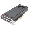
In this review, we're taking a close look at the AMD reference design of the Radeon RX 480. The dual-slot card comes with a single-fan-blower cooler in the traditional AMD style and just a 6-pin power input. Pricing has been set at $239 for the 8 GB version we are reviewing today, and there soon will also be a 4 GB version for $199, though its memory clocks will be lower.
| Radeon R9 380X | GeForce GTX 780 | Radeon R9 290 | Radeon R9 390 | GeForce GTX 970 | Radeon RX 480 | Radeon R9 290X | Radeon R9 390X | GeForce GTX 780 Ti | GeForce GTX 980 | Radeon R9 Fury | |
|---|---|---|---|---|---|---|---|---|---|---|---|
| Shader Units | 2048 | 2304 | 2560 | 2560 | 1664 | 2304 | 2816 | 2816 | 2880 | 2048 | 3584 |
| ROPs | 32 | 48 | 64 | 64 | 56 | 32 | 64 | 64 | 48 | 64 | 64 |
| Graphics Processor | Tonga | GK110 | Hawaii | Hawaii | GM204 | Ellesmere | Hawaii | Hawaii | GK110 | GM204 | Fiji |
| Transistors | unknown | 7100M | 6200M | 6200M | 5200M | 5700M | 6200M | 6200M | 7100M | 5200M | 8900M |
| Memory Size | 4 GB | 3 GB | 4 GB | 8 GB | 4 GB | 8 GB | 4 GB | 8 GB | 3 GB | 4 GB | 4 GB |
| Memory Bus Width | 256 bit | 384 bit | 512 bit | 512 bit | 256 bit | 256 bit | 512 bit | 512 bit | 384 bit | 256 bit | 4096 bit |
| Core Clock | 970 MHz | 863 MHz+ | 947 MHz | 1000 MHz | 1051 MHz+ | 1120 - 1266 MHz | 1000 MHz | 1050 MHz | 876 MHz+ | 1126 MHz+ | 1000 MHz |
| Memory Clock | 1425 MHz | 1502 MHz | 1250 MHz | 1500 MHz | 1750 MHz | 2000 MHz | 1250 MHz | 1500 MHz | 1750 MHz | 1750 MHz | 500 MHz |
| Price | $210 | $290 | $235 | $260 | $265 | $239 | $270 | $310 | $390 | $360 | $530 |
Architecture
At the heart of the Radeon RX 480 is the new "Ellesmere" (Polaris 10) GPU built on the 14 nanometer silicon fab process by Samsung and GlobalFoundries. The wafers are made in Upstate New York, USA, and are then bumped and packaged at a facility in Taiwan to be sent to the various graphics card manufacturers located there and across the straits.

This GPU is based on AMD's fourth generation Graphics CoreNext architecture codenamed "Polaris." According to AMD, Compute Units (CUs) based on Polaris are 15% more efficient at number-crunching than CUs based on the preceding Graphics CoreNext 1.2 architecture (R9 Fury, R9 380X). Pay attention to the numbers here. While the number-crunching machinery is 15% more efficient, the chip overall is claimed to have a 2.5x leap in energy-efficiency over the previous generation. This is because AMD is cashing in on the immediate gains a new silicon fab process brings to the table, the 14 nm FinFET process in this case, to increase transistor counts and clock speeds.

The component hierarchy in the Polaris 10 "Ellesmere" silicon is similar to older-generation chips, although each of the components received major updates. We begin with the chip featuring two hardware schedulers and the introduction of dedicated real-time asynchronous compute with spatial and temporal scheduling. The chip features four async compute engines (ACEs). AMD optimized the async compute engine with new quick-response queue tech.


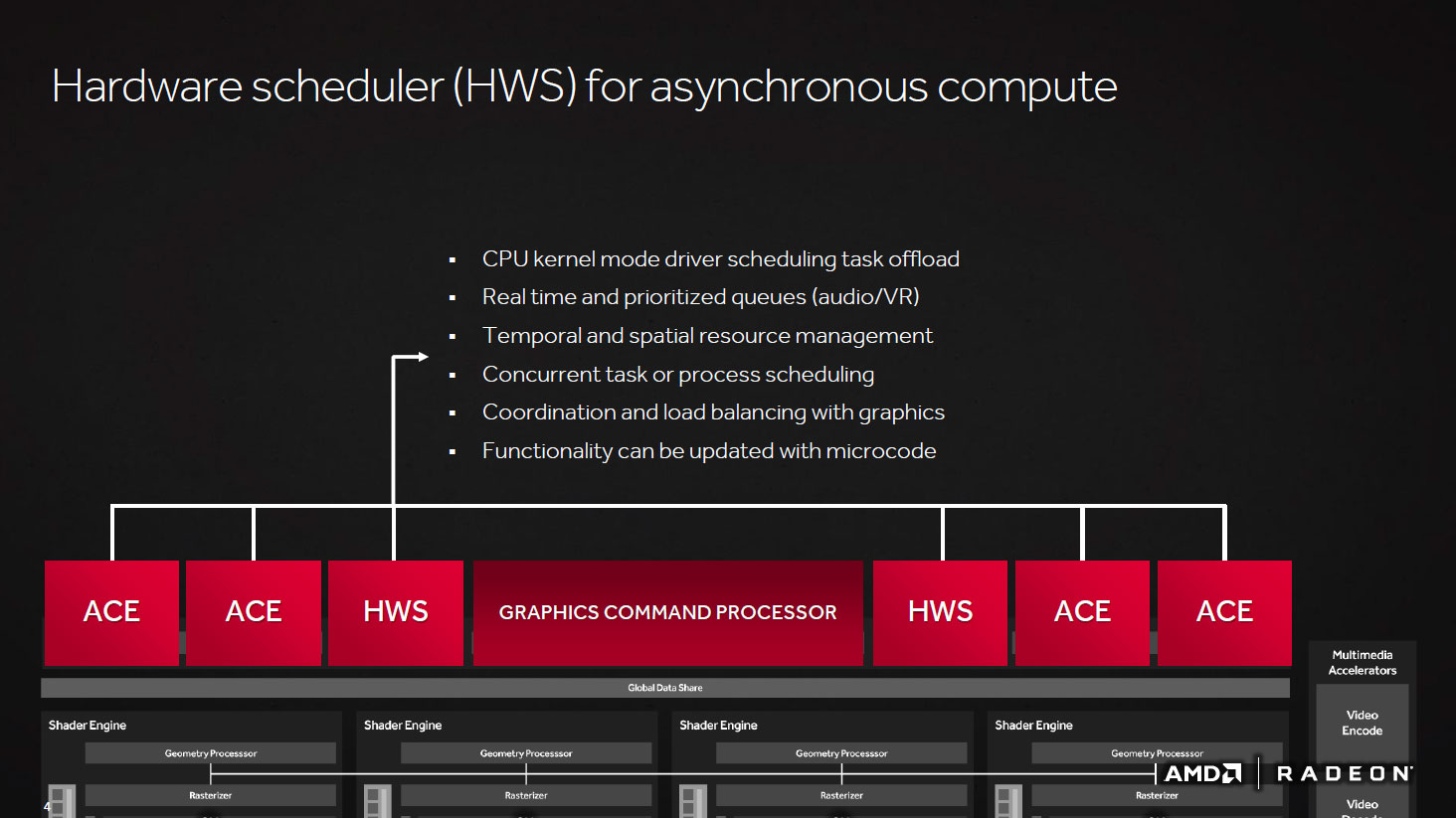
There's a design focus on stepping up geometry processing performance and blunting the brute-tessellation advantage NVIDIA traditionally enjoyed over AMD. For a chip of this segment, Polaris 10 features four independent geometry processors. Their functionality is upgraded over the previous generation, featuring a primitive discard accelerator which culls (discards) triangles in the pipeline with zero area or no inclusive sample points. The geometry engine now features a tiny cache called the Index Cache, which cushions small instanced geometry and reduces data movement, improving primitive throughput during instancing.
The Polaris 10 silicon features 36 Compute Units (CUs), spread across four shader engines, each with a dedicated geometry processor, a raster engine, and two render backends. The four shader engines are supported by a large 2 MB L2 cache, which acts as the town-square for the various key components of the GPU.
Most of the architecture-specific innovations are centered on the CU, which now features a hardware instruction prefetcher, a larger instruction buffer, and native half-precision (FP16/Int16) support, which should reliably crunch numbers for gaming applications with significantly reduced memory and register footprints while lowering power execution. Altogether, the "Polaris" CU is claimed to have up to 15% higher performance than CUs based on the GCN 1.1 architecture (R9 390X). Each CU features 64 stream processors, and so the 36 CUs amount to 2,304 stream processors. The Radeon RX 480 maxes out all CUs physically present on the chip. In summary, the Polaris 10 chip features 2,304 stream processors, 144 TMUs, and 32 ROPs.


The Polaris 10 chip features a 256-bit wide GDDR5 memory interface, supporting 8 Gbps memory chips in sizes of up to 8 GB. The actual memory bandwidth of this interface, at its given clock speeds, is rated at up to 256 GB/s, although its effective bandwidth could be higher thanks to an updated lossless delta color compression (DCC) tech with full 2/4/8:1 compression ratios. AMD claims that its new gen DCC tech can provide an effective bandwidth uplift of a staggering 30 percent.


The multimedia accelerators receive a major update, now supporting H.265 Main10 decode hardware acceleration and 4K60 HEVC encode hardware acceleration. The other components with big updates are the display controllers, which now support DisplayPort 1.4 (DP 1.3 HBR3 and DP 1.4 HDR) and HDMI 2.0b. FreeSync is supported over both DP and HDMI. Resolutions as high as 5K60, 10-bit 4K96 HDR, and 4K120 SDR are supported.
The Card

AMD's reference design follows the style introduced with the Fury X; a backplate is not available (which is not unreasonable in this performance class). Dimensions of the card are 24.5 cm x 11.0 cm.

Installation requires two slots in your system.

Display connectivity options include three DisplayPorts and one HDMI port. With the AMD Fury Series, AMD removed support for analog output in the DVI port connector, and now, the DVI connector has been removed completely. The HDMI port is now version 2.0b and DisplayPort has been updated to 1.3 HBR3/1.4 HDR ready, which enables support for 4K at 120 Hz and 5K @ 60 Hz, or 8K @ 60 Hz with two cables.
GPU accelerated encoding is now supported for H.264 at up to 4K30, and HEVC is supported at up to 4K60. Accelerated decoding is supported for HEVC at up to 4K60 Main-10, VP9 is supported at up to 4K, and H.264 at up to 4K120.

AMD CrossFire has been running over the PCI-Express bus for a few generations now. The Polaris Series is no different. CrossFire is supported at up to 4x configurations.

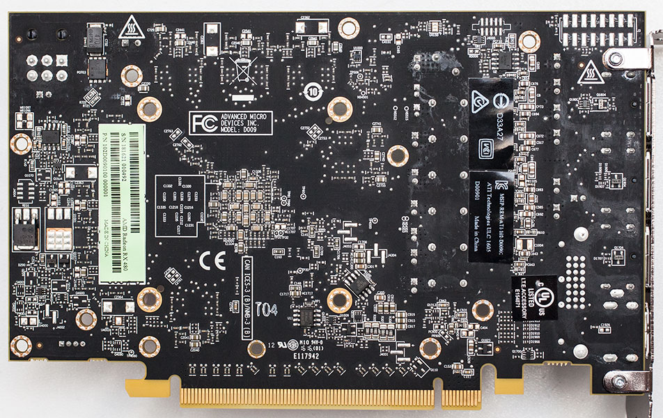
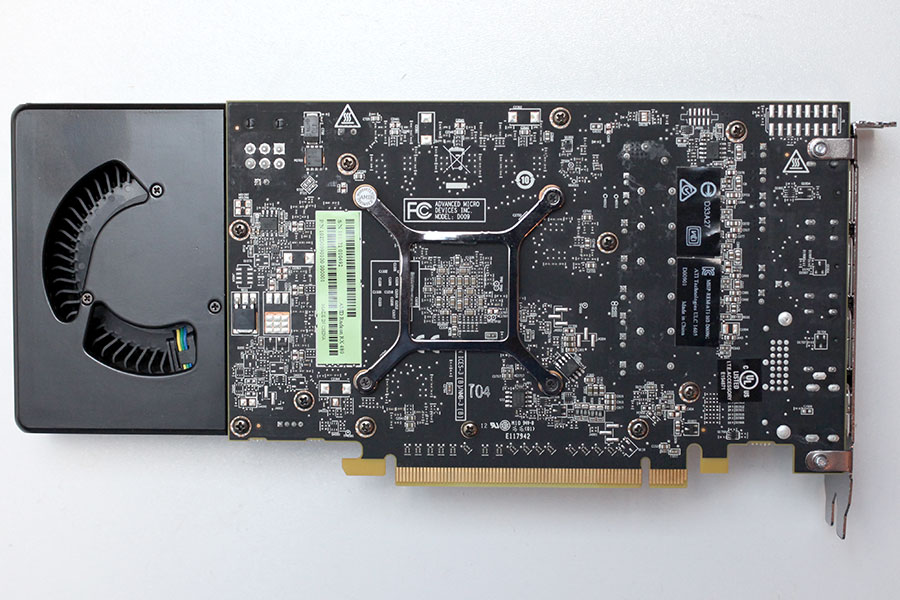
Pictured above are the front and back, showing the disassembled board. High-res versions are also available (front, back).
A Closer Look


The AMD heatsink does not use any heapipes. A large block of metal with a copper core sits in the airflow generated by the fan. You can also see thermal pads that provide cooling for the VRM circuitry and memory chips.

AMD is using one additional 6-pin power connector. This input configuration is specified for up to 150 watts of power draw.
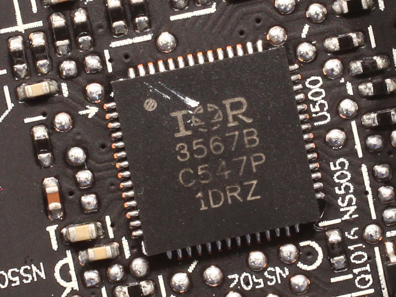
We've seen the IR3567 voltage controller on several designs from AMD before. It has support for I2C voltage control and advanced monitoring.

The GDDR5 memory chips are made by Samsung and carry the model number K4G80325FB-HC25. They are specified to run at 2000 MHz (8000 MHz GDDR5 effective).
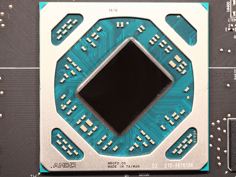
AMD's Ellesmere graphics processor introduces the company's Polaris architecture. It is produced on a 14 nm process at Globalfoundries, USA, with a transistor count of 5.7 billlion and a die size of 232 mm².
Our Patreon Silver Supporters can read articles in single-page format.
Jul 12th, 2025 05:19 CDT
change timezone
Latest GPU Drivers
New Forum Posts
- Gigabyte graphic cards - TIM gel SLIPPAGE problem (146)
- What's your latest tech purchase? (24240)
- Best motherboards for XP gaming (103)
- ASUS ProArt GeForce RTX 4060 Ti OC Edition 16GB GDDR6 Gaming - nvflash64 VBIOS mismatch (3)
- Steam Deck Owners Clubhouse (535)
- What are you playing? (23923)
- Chrome has removed uBlock Origin 1.64.0 (remove google search suggestions) (0)
- Can you guess Which game it is? (227)
- Will you buy a RTX 5090? (645)
- 'NVIDIA App' not usable offline? (9)
Popular Reviews
- Fractal Design Epoch RGB TG Review
- Corsair FRAME 5000D RS Review
- Lexar NM1090 Pro 4 TB Review
- NVIDIA GeForce RTX 5050 8 GB Review
- NZXT N9 X870E Review
- Sapphire Radeon RX 9060 XT Pulse OC 16 GB Review - An Excellent Choice
- Our Visit to the Hunter Super Computer
- AMD Ryzen 7 9800X3D Review - The Best Gaming Processor
- Upcoming Hardware Launches 2025 (Updated May 2025)
- Chieftec Iceberg 360 Review
TPU on YouTube
Controversial News Posts
- Intel's Core Ultra 7 265K and 265KF CPUs Dip Below $250 (288)
- Some Intel Nova Lake CPUs Rumored to Challenge AMD's 3D V-Cache in Desktop Gaming (140)
- AMD Radeon RX 9070 XT Gains 9% Performance at 1440p with Latest Driver, Beats RTX 5070 Ti (131)
- NVIDIA Launches GeForce RTX 5050 for Desktops and Laptops, Starts at $249 (119)
- NVIDIA GeForce RTX 5080 SUPER Could Feature 24 GB Memory, Increased Power Limits (115)
- Microsoft Partners with AMD for Next-gen Xbox Hardware (105)
- Intel "Nova Lake‑S" Series: Seven SKUs, Up to 52 Cores and 150 W TDP (100)
- NVIDIA DLSS Transformer Cuts VRAM Usage by 20% (97)